Source
engines/atom_fishbone_coupler/notes/2026-07-27_unit_cell_geometry.md · assembled 2026-07-29 15:57 UTC.
2026-07-27 — Unit cell geometry schematic (pre-simulation)
Latest simulation status — Stage 2 3D MPB
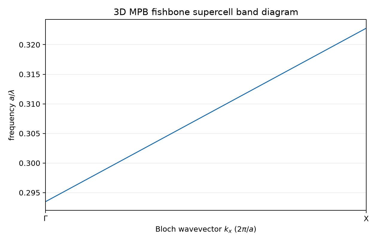
Completed: first 3D MPB Γ–X band-edge baseline for the requested fishbone
(a = 0.23 µm, t = 0.30 µm, W = 1.20 µm, w_slot = 1.00 µm,
A = 0.50 µm). The target-near branch is at a/λ = 0.293477 (783.7 nm) at
Γ and 0.322780 (712.6 nm) at X. This is a coarse one-branch baseline, not a
converged full bandgap calculation. Full details and raw artifacts appear in
the Stage 2 entry later on this page.
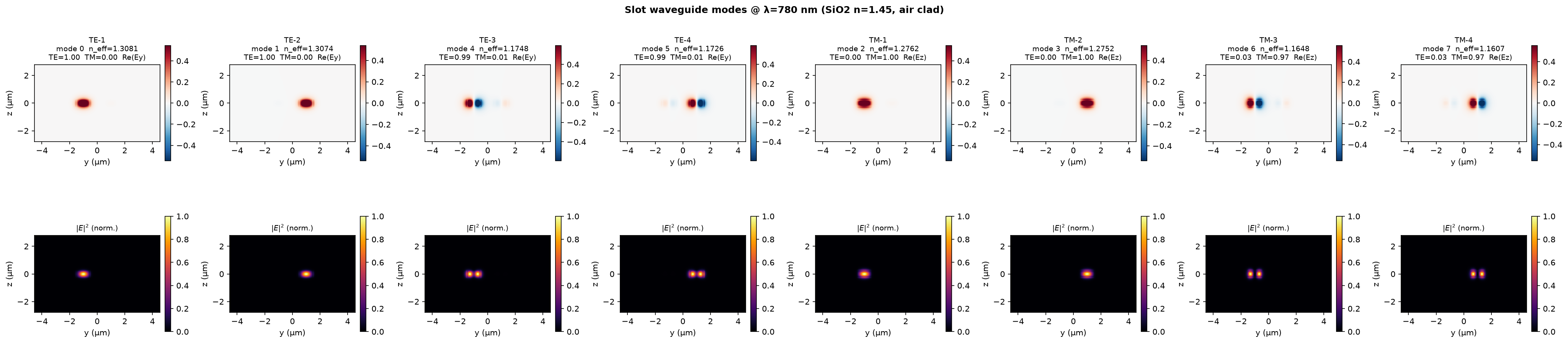
Latest 2D material check: an SiO₂/air slot guide with a 1.0 µm air gap does support ordinary guided modes, but none is air-gap dominant; the strongest sampled gap electric-intensity fraction is only 8.2%. Details appear in the SiO₂ entry later on this page.
Why
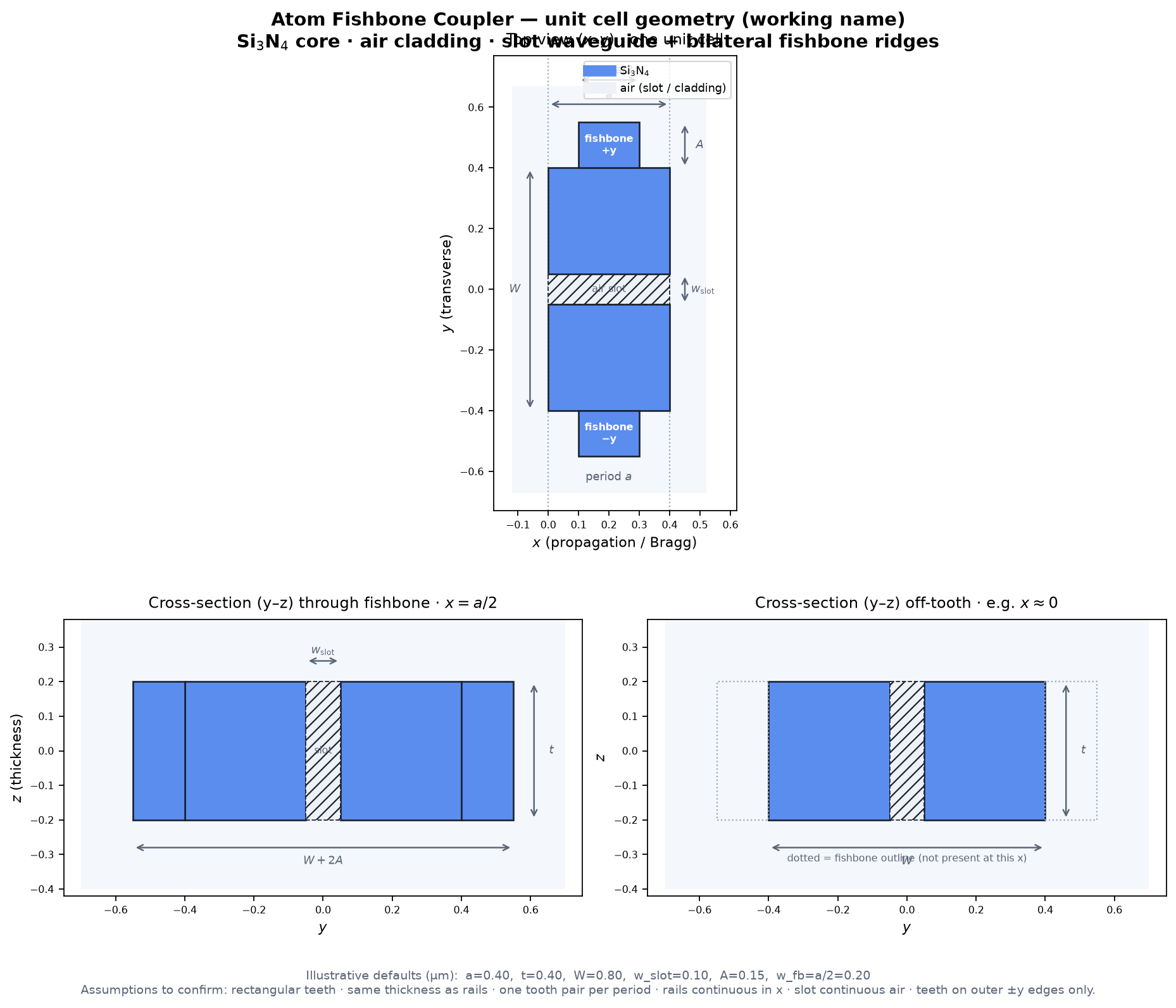
New engine Atom Fishbone Coupler (working name) created from scratch — not a fork. Before any MPB run, lock a shared picture of the unit cell.
Materials
- Core: Si₃N₄
- Cladding: air
Parameters (symbols)
| Symbol | Meaning |
|---|---|
a |
Bragg / unit-cell period along x |
t |
Film thickness along z |
W |
Total slot-waveguide width (outer rail edge to outer rail edge), not including fishbone amplitude |
w_slot |
Air slot width (centered at y = 0) |
A |
Fishbone amplitude — how far each tooth protrudes beyond the rail in ±y (both sides) |
w_fb |
Fishbone tooth width along x; default a/2 |
Derived: each rail width = (W − w_slot) / 2.
Construction (my understanding)
One period 0 ≤ x < a, structure centered on y = 0, midplane z = 0:
- Left rail (Si₃N₄): full period in x,
y ∈ [−W/2, −w_slot/2],z ∈ [−t/2, t/2] - Right rail (Si₃N₄): full period in x,
y ∈ [+w_slot/2, +W/2],z ∈ [−t/2, t/2] - Fishbone +y (Si₃N₄): rectangle, width
w_fb(default centered →[a/4, 3a/4]ifw_fb = a/2),y ∈ [W/2, W/2+A], samez - Fishbone −y (Si₃N₄): mirror,
y ∈ [−W/2−A, −W/2] - Everything else in the cell: air (including the continuous slot)
Assumptions flagged for review
- Teeth are rectangular and same thickness as the rails.
- One tooth pair per period, centered in x.
- Rails are continuous in x; only outer ±y edges grow teeth.
- Slot is continuous air (no Si₃N₄ bridge across the slot).
Wdoes not include amplitudeA(outer extent isW/2 + A).- Illustrative numerical defaults in the figure are for readability only.
Schematic
Artifacts
| File | Role |
|---|---|
schematics/unit_cell.yaml |
Parameter + construction definition |
schematics/draw_unit_cell.py |
Schematic generator |
figures/unit_cell_schematic.png |
Multi-view figure (top + two yz cuts) |
figures/unit_cell_schematic.svg |
Vector copy |
Regenerate:
2D slot-waveguide modes @ 780 nm (no fishbone)
Geometry confirmed schematically; first solver step is the plain slot only (no fishbone teeth), as a 2D y–z cross-section eigenmode problem with propagation along x.
Why Tidy3D (not MPB yet)
- MPB is not installed on this host yet, and geometry/units need extra care (overlapping shapes, scale free units).
- Tidy3D’s local
ModeSolveris available (tidy3d 2.11.2) and does not need a cloud API key for this cross-section solve. - Full Bragg unit cell / band diagram still planned for MPB after this baseline.
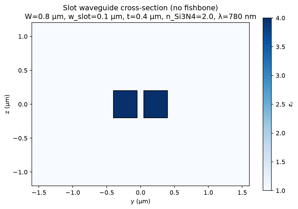
Geometry (µm) — same defaults as the schematic rails
| Parameter | Value |
|---|---|
| λ | 780 nm (0.78 µm) |
| W | 0.80 |
| w_slot | 0.10 |
| t | 0.40 |
| n_Si₃N₄ | 2.00 (constant; dispersion model not chosen yet) |
| cladding | air (n = 1) |
| fishbone | omitted |
Cross-section used by the solver
Mode classification
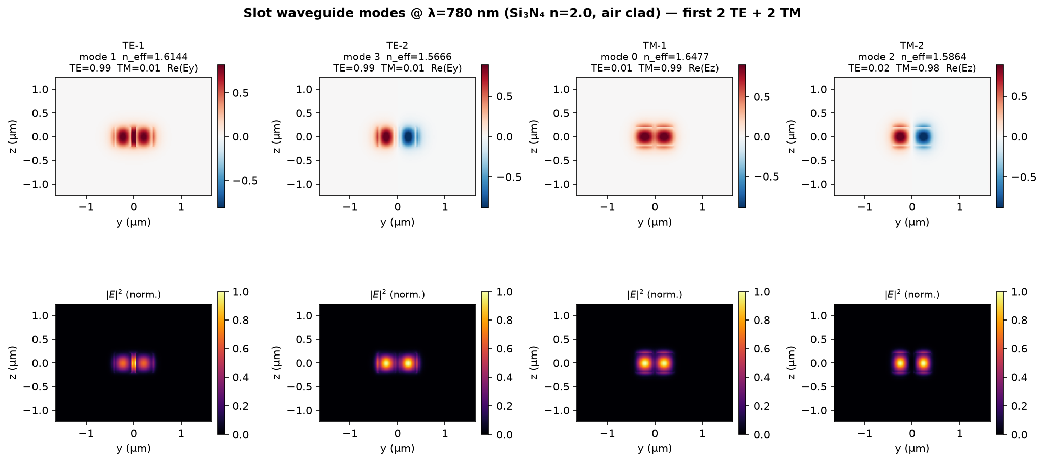
Tidy3D reports pol_fraction.te / .tm on the mode plane (y–z). We keep the
first 2 TE-like and 2 TM-like modes with highest fraction of each
polarization among the bound-ish spectrum (num_modes=12, min_steps_per_wvl=30).
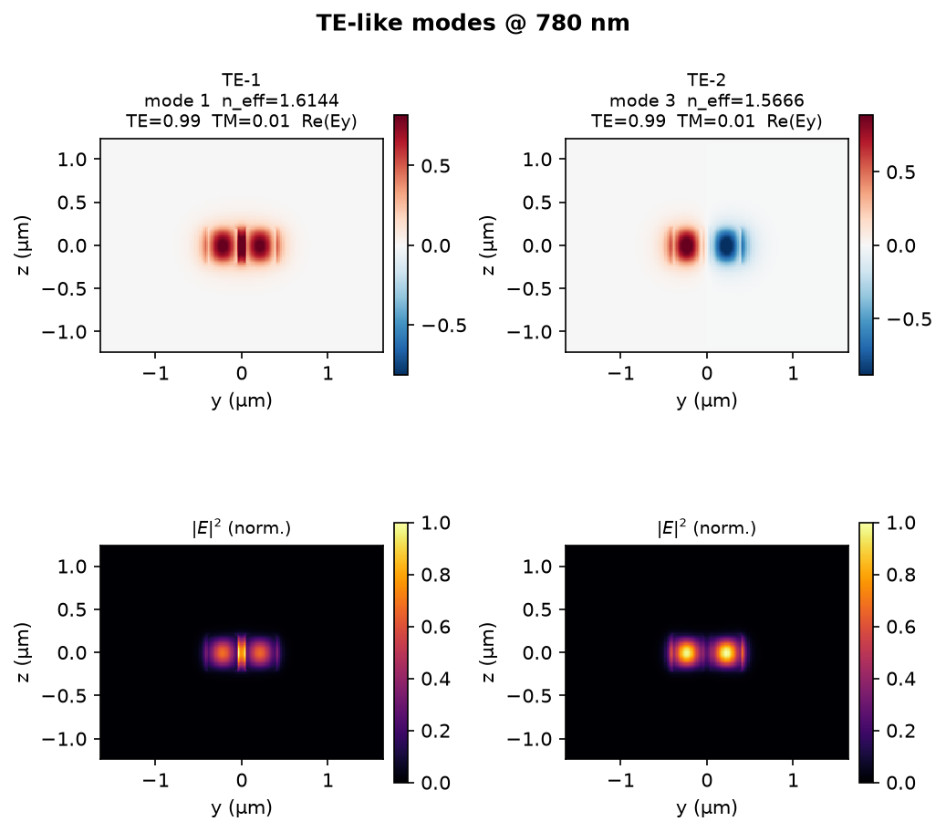
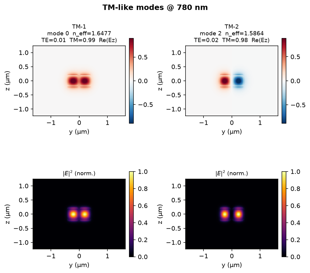
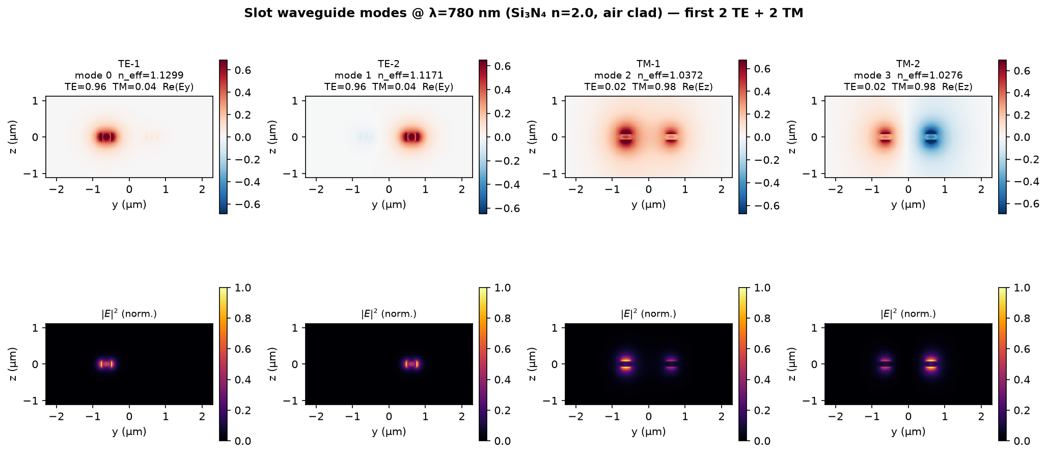
Plot convention: TE panels show Re(Ey) (in-plane, across the slot); TM panels show Re(Ez) (out-of-plane). Bottom row is normalized |E|².
Results (n_eff @ 780 nm)
| Label | mode index | n_eff | TE frac | TM frac | character (from fields) |
|---|---|---|---|---|---|
| TM-1 | 0 | 1.6477 | 0.01 | 0.99 | even Ez on both rails (fundamental) |
| TE-1 | 1 | 1.6144 | 0.99 | 0.01 | Ey enhanced in the slot (even-ish) |
| TM-2 | 2 | 1.5864 | 0.02 | 0.98 | odd Ez (left/right opposite) |
| TE-2 | 3 | 1.5666 | 0.99 | 0.01 | odd Ey (left/right opposite) |
Note: for these dimensions the fundamental is TM-like (highest n_eff), with the first TE-like slot mode second. Higher modes with n_eff ≲ 1.2 look weakly confined / continuum-adjacent; modes 9–11 warned about boundary decay.
Mode shapes (first 2 TE + 2 TM)
Separate panels:
Artifacts (this step)
| File | Role |
|---|---|
package/atom_fishbone/slot_waveguide_modes_2d.py |
local ModeSolver driver + plots |
runs/slot_waveguide_modes_2d_780nm/summary.json |
n_eff / pol fractions for all modes |
figures/slot_waveguide_cross_section_2d.png |
ε_r cross-section |
figures/slot_waveguide_modes_2d_780nm.png |
combined TE+TM field panel |
figures/slot_waveguide_TE_modes_2d_780nm.png |
TE only |
figures/slot_waveguide_TM_modes_2d_780nm.png |
TM only |
Regenerate:
python engines/atom_fishbone_coupler/package/atom_fishbone/slot_waveguide_modes_2d.py
python tools/build_docs_site.py
Caveats
- n_Si₃N₄ = 2.0 is a flat placeholder at 780 nm (real Si₃N₄ is slightly dispersive / process-dependent).
- Local ModeSolver warned that remote/subpixel averaging is more accurate; numbers are good for shapes and ordering, not final design tolerances.
- TE/TM labels follow Tidy3D plane polarization fractions, not every paper’s “quasi-TE” naming for slots — fields are the source of truth.
- Fishbone is not in this solve. Next physics step: MPB band diagram of the full periodic unit cell (after MPB install + careful non-overlapping geometry).
Still open / next
- Confirm n_Si₃N₄ model (constant vs dispersive).
- Install MPB and build the fishbone unit cell carefully (no ambiguous overlaps; consistent scale to µm or a).
- Band diagram of the Bragg unit cell; compare gap / guided bands to this slot baseline.
2D slot modes — t = 150 nm, W = 1.5 µm, w_slot = 1.0 µm @ 780 nm
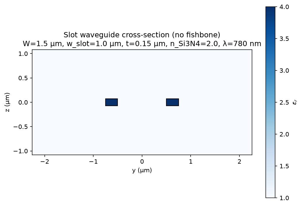
Same solver as above (Tidy3D local ModeSolver, y–z cross-section, no fishbone). New geometry requested:
| Parameter | Value |
|---|---|
| λ | 780 nm |
| t | 150 nm (0.15 µm) |
| W | 1.5 µm |
| w_slot | 1.0 µm |
| rail width each | (W − w_slot)/2 = 0.25 µm |
| n_Si₃N₄ | 2.00 (constant) |
| cladding | air |
Cross-section
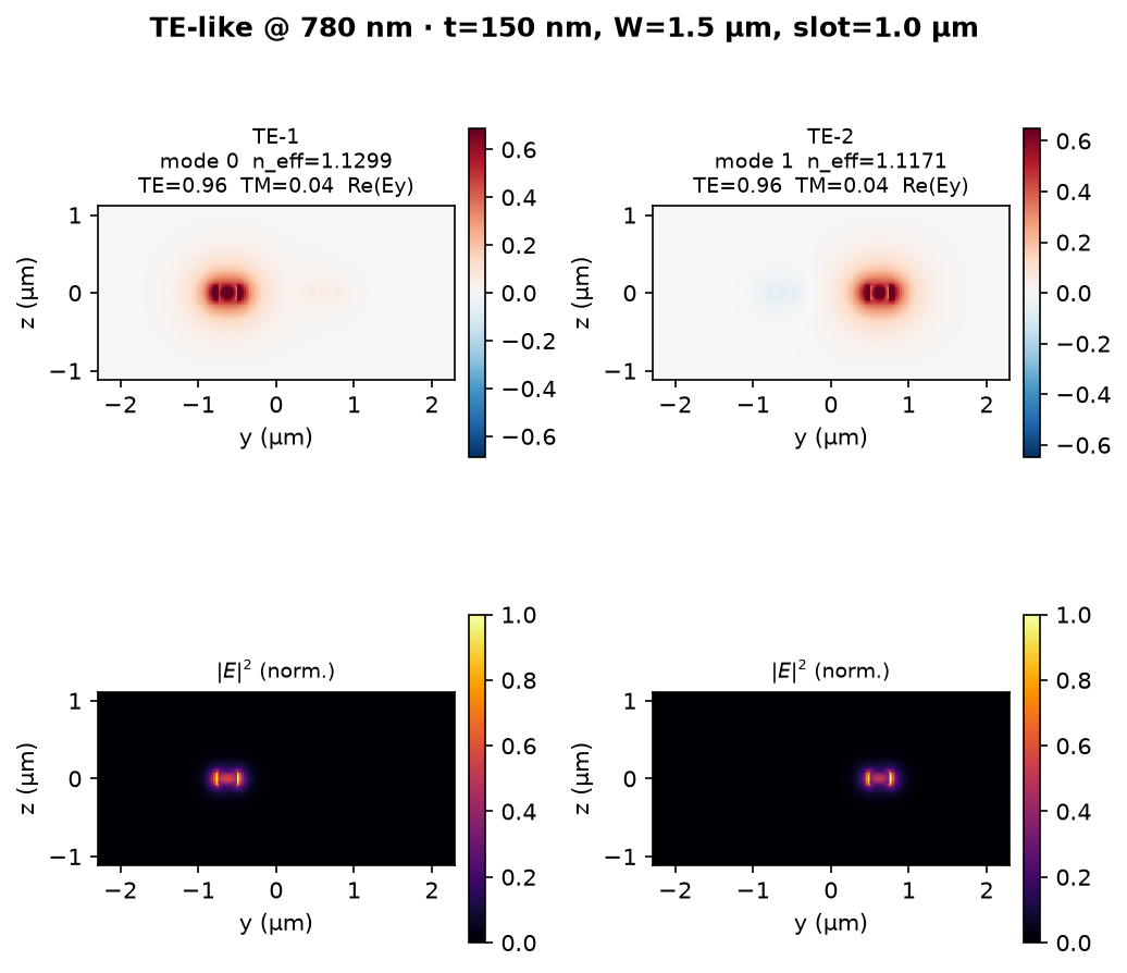
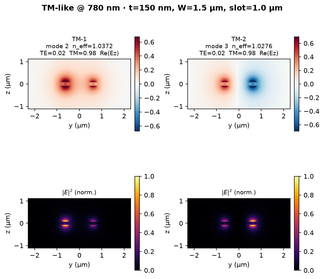
Results (n_eff ≥ 1 preferred; first 2 TE + 2 TM by n_eff within pol)
| Label | mode index | n_eff | TE frac | TM frac |
|---|---|---|---|---|
| TE-1 | 0 | 1.1299 | 0.96 | 0.04 |
| TE-2 | 1 | 1.1171 | 0.96 | 0.04 |
| TM-1 | 2 | 1.0372 | 0.02 | 0.98 |
| TM-2 | 3 | 1.0276 | 0.02 | 0.98 |
Compared with the earlier thicker / narrower-slot baseline (t=400 nm, W=0.8, w_slot=0.1), n_eff values are much lower here: thin film + wide 1 µm air gap + only 0.25 µm rails → weakly confined modes sitting just above the air light line. Modes with n_eff ≲ 1 (indices ≥ 4) do not decay at the mode-plane boundaries (continuum / leaky).
For this geometry the two highest-n_eff modes are TE-like, then two TM-like (opposite of the previous baseline, where TM was fundamental).
Mode shapes
Artifacts
| File | Role |
|---|---|
runs/slot_waveguide_modes_2d_t150nm_W1p5_slot1p0_780nm/summary.json |
full spectrum + picks |
figures/slot_waveguide_*_t150nm_W1p5_slot1p0_780nm.png |
cross-section + field panels |
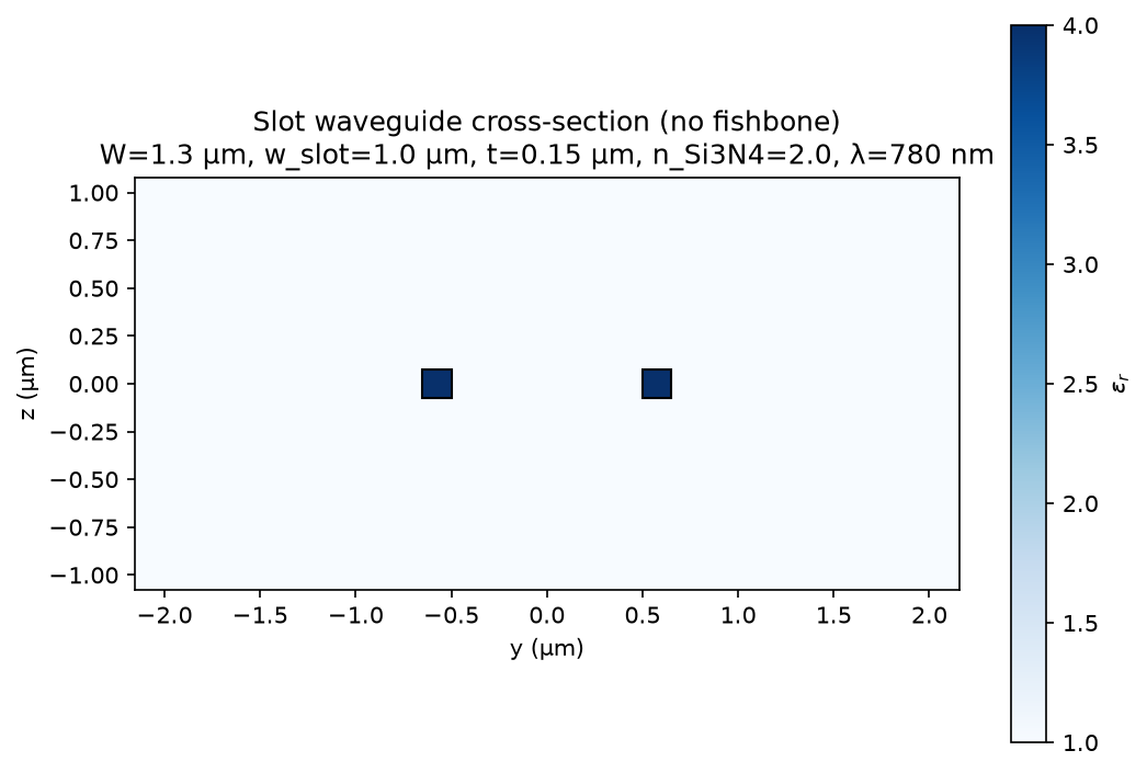
2D slot modes — t = 150 nm, W = 1.3 µm, w_slot = 1.0 µm @ 780 nm
Same solver; thinner rails than the previous W=1.5 case.
| Parameter | Value |
|---|---|
| λ | 780 nm |
| t | 150 nm |
| W | 1.3 µm |
| w_slot | 1.0 µm |
| rail width each | (W − w_slot)/2 = 0.15 µm |
| n_Si₃N₄ | 2.00 |
| cladding | air |
Cross-section
Results (first 2 TE + 2 TM by n_eff within pol)
| Label | mode index | n_eff | TE frac | TM frac | note |
|---|---|---|---|---|---|
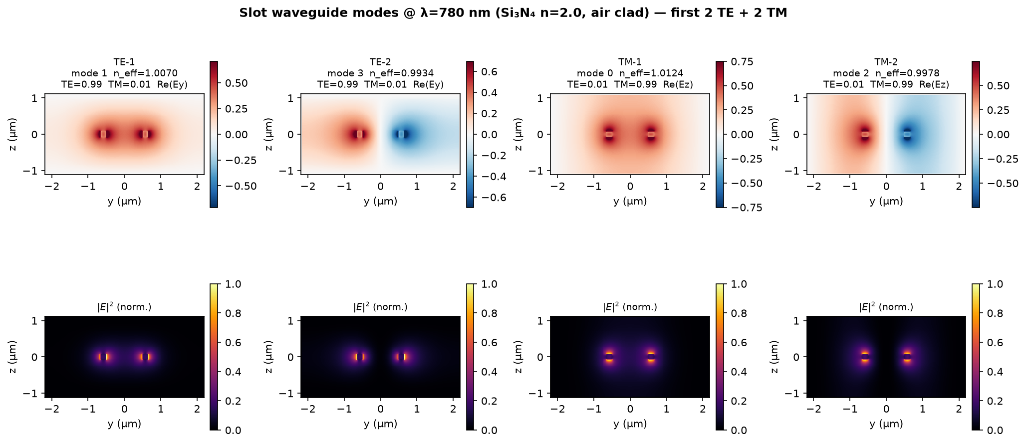
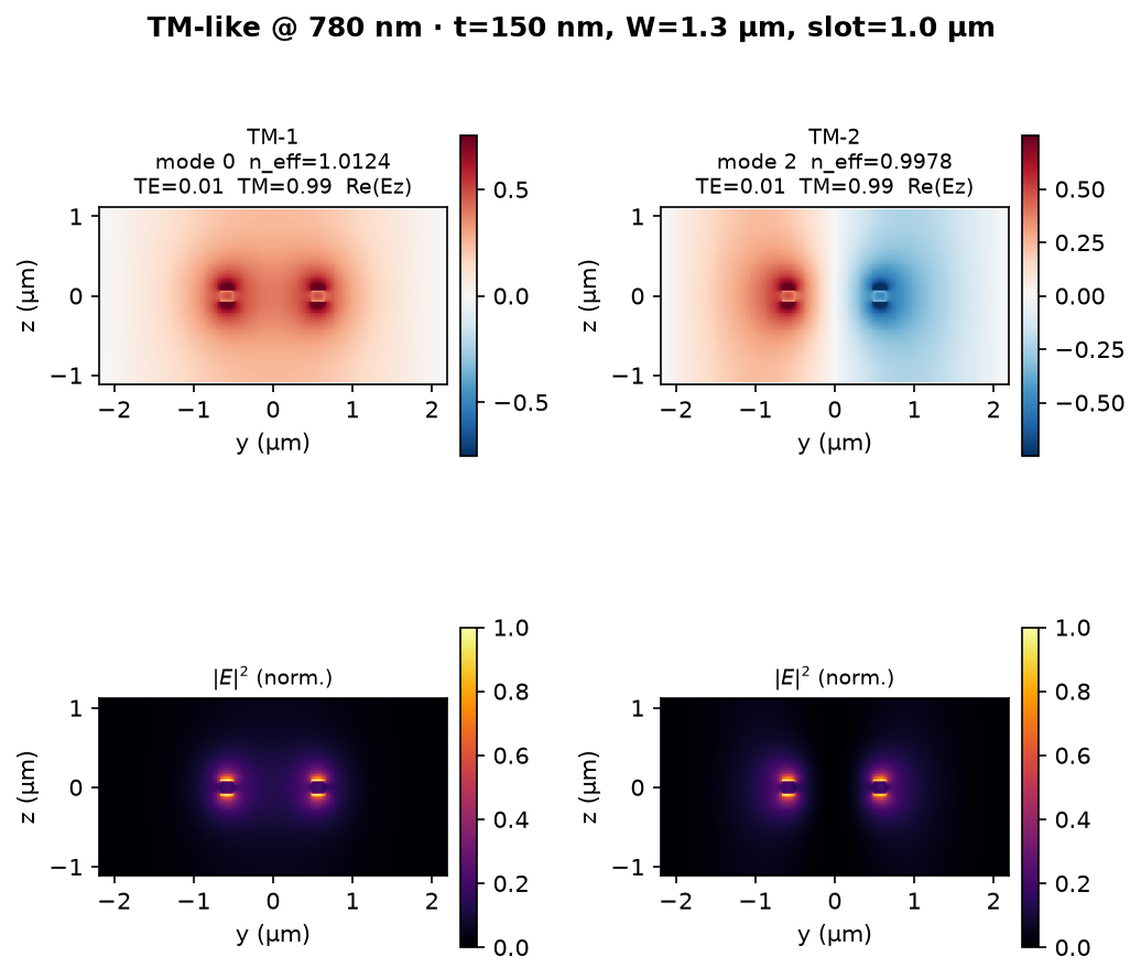
| TM-1 | 0 | 1.0124 | 0.01 | 0.99 | only TM above air light line |
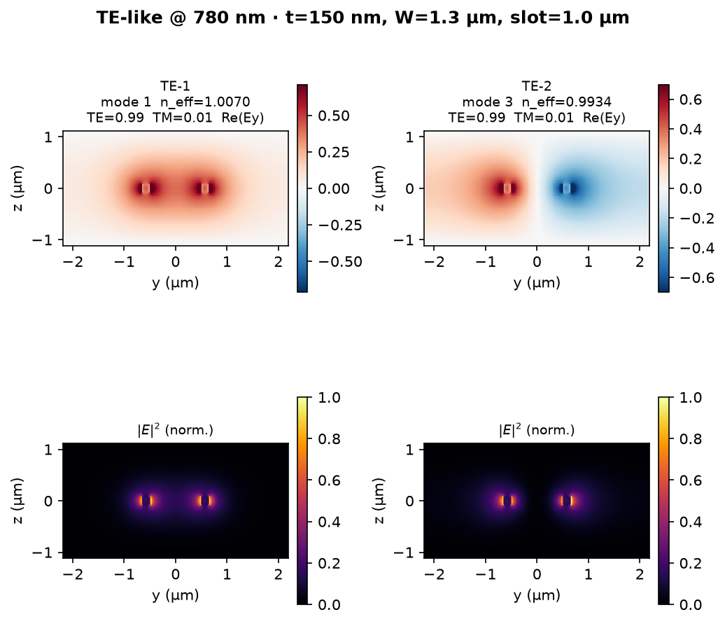
| TE-1 | 1 | 1.0070 | 0.99 | 0.01 | only TE above air light line |
| TM-2 | 2 | 0.9978 | 0.01 | 0.99 | just below n = 1 |
| TE-2 | 3 | 0.9934 | 0.99 | 0.01 | just below n = 1 |
Only two modes sit at n_eff ≥ 1 (TM-1, TE-1). Compared with W=1.5 µm (rails 0.25 µm), shrinking total width to 1.3 µm (rails 0.15 µm) drops n_eff further toward cutoff. Higher modes again fail to decay at the mode-plane boundaries.
Mode shapes
Artifacts
| File | Role |
|---|---|
runs/slot_waveguide_modes_2d_t150nm_W1p3_slot1p0_780nm/summary.json |
spectrum + picks |
figures/slot_waveguide_*_t150nm_W1p3_slot1p0_780nm.png |
plots |
2D slot modes — t = 150 nm, W = 1.3 µm, w_slot = 0.5 µm @ 780 nm
| Parameter | Value |
|---|---|
| λ | 780 nm |
| t | 150 nm |
| W | 1.3 µm |
| w_slot | 0.5 µm |
| rail width each | 0.40 µm |
| n_Si₃N₄ | 2.00 |
n_eff
| Label | mode | n_eff | TE frac | TM frac |
|---|---|---|---|---|
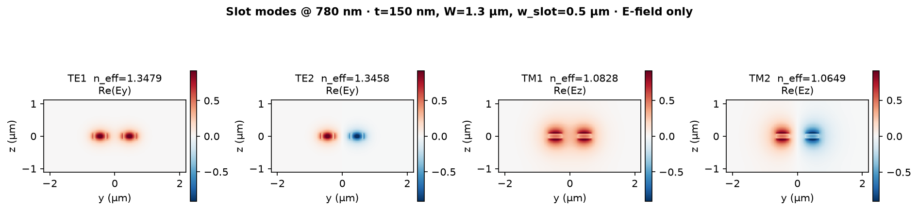
| TE1 | 0 | 1.3479 | 0.98 | 0.02 |
| TE2 | 1 | 1.3458 | 0.98 | 0.02 |
| TM1 | 2 | 1.0828 | 0.02 | 0.98 |
| TM2 | 3 | 1.0649 | 0.03 | 0.97 |
Halving the gap vs 1.0 µm raises TE n_eff substantially (~1.35) and pulls both TE and TM clearly above the air light line. TE is fundamental (pair of nearly degenerate even/odd-like TE supermodes).
E-field only (TE1, TE2, TM1, TM2)
Re(Ey) for TE, Re(Ez) for TM — no intensity plots.
Artifacts
runs/slot_waveguide_modes_2d_t150nm_W1p3_slot0p5_780nm/summary.jsonfigures/slot_waveguide_Efields_TE_TM_t150nm_W1p3_slot0p5_780nm.png
TE1–4 and TM1–4 E-fields (same geometry)
Extended request: also show TE3, TE4, TM3, TM4. Still Re(E) only (Ey for TE, Ez for TM).
| Label | mode | n_eff | note |
|---|---|---|---|
| TE1 | 0 | 1.3479 | guided |
| TE2 | 1 | 1.3458 | guided |
| TE3 | 5 | 0.9843 | n_eff < 1 (leaky / continuum-adjacent) |
| TE4 | 6 | 0.9775 | n_eff < 1 |
| TM1 | 2 | 1.0828 | guided |
| TM2 | 3 | 1.0649 | guided |
| TM3 | 4 | 0.9856 | n_eff < 1 |
| TM4 | 7 | 0.9761 | n_eff < 1 |
Only four modes sit above the air light line (TE1–2, TM1–2). TE3–4 and TM3–4 are the next TE/TM-classified modes by n_eff; fields do not fully decay at the solver window edges.
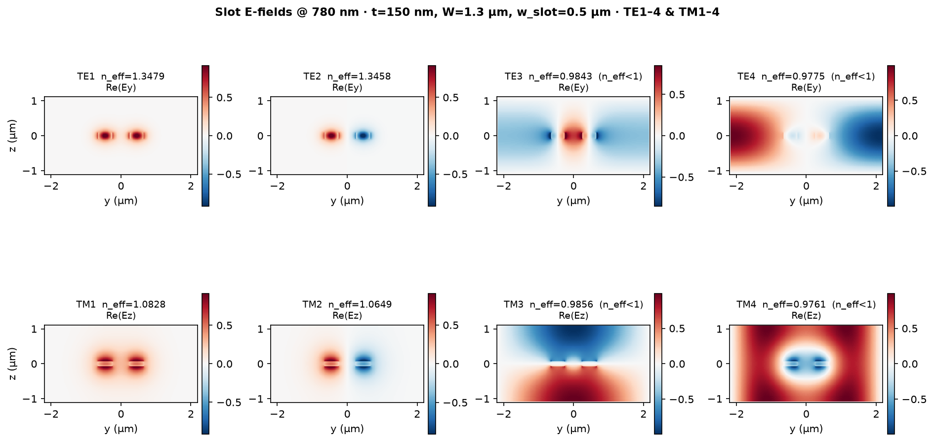
Artifact: figures/slot_waveguide_Efields_TE1-4_TM1-4_t150nm_W1p3_slot0p5_780nm.png
2D slot modes — t = 150 nm, W = 1.0 µm, w_slot = 0.5 µm @ 780 nm
| Parameter | Value |
|---|---|
| λ | 780 nm |
| t | 150 nm |
| W | 1.0 µm |
| w_slot | 0.5 µm |
| rail width each | 0.25 µm |
| n_Si₃N₄ | 2.00 |
TE1–4 and TM1–4 (E-field only)
| Label | mode | n_eff | note |
|---|---|---|---|
| TE1 | 0 | 1.1336 | guided |
| TE2 | 1 | 1.0998 | guided |
| TE3 | 5 | 0.9762 | n_eff < 1 |
| TE4 | 6 | 0.9749 | n_eff < 1 |
| TM1 | 2 | 1.0442 | guided |
| TM2 | 3 | 1.0108 | guided |
| TM3 | 4 | 0.9811 | n_eff < 1 |
| TM4 | 7 | 0.9710 | n_eff < 1 |
Compared with W=1.3 µm / same gap: TE n_eff drops (1.35 → ~1.13) as rails shrink from 0.40 → 0.25 µm. Still four modes above air light line (TE1–2, TM1–2).
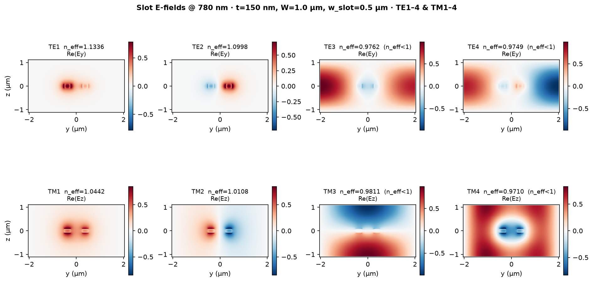
Artifacts
runs/slot_waveguide_modes_2d_t150nm_W1p0_slot0p5_780nm/summary.jsonfigures/slot_waveguide_Efields_TE1-4_TM1-4_t150nm_W1p0_slot0p5_780nm.png
2D slot modes — t = 0.30 µm, W = 1.0 µm, w_slot = 0.5 µm @ 780 nm
Same lateral geometry as the previous W=1.0 / gap=0.5 case; thickness raised to 300 nm.
| Parameter | Value |
|---|---|
| λ | 780 nm |
| t | 0.30 µm |
| W | 1.0 µm |
| w_slot | 0.5 µm |
| rail width each | 0.25 µm |
First truly guided mode (n_eff > 1, air-clad)
Criterion used here: n_eff > n_air = 1 (bound vs continuum for air cladding).
| First guided | TM1 (solver mode 0) |
| n_eff | 1.3964 |
| pol | TM fraction 0.98 |
All guided (n_eff > 1), ordered by n_eff:
| rank | label | mode | pol | n_eff |
|---|---|---|---|---|
| 1 | TM1 | 0 | TM | 1.3964 |
| 2 | TM2 | 1 | TM | 1.3625 |
| 3 | TE1 | 2 | TE | 1.3297 |
| 4 | TE2 | 3 | TE | 1.2809 |
So with t = 0.30 µm the fundamental is TM, not TE (unlike the thinner t = 0.15 µm case at the same W/gap, where TE led). TE3–4 and TM3–4 remain below the light line.
E-fields TE1–4 & TM1–4
Green border on the panel marks the first guided mode. Re(Ey) for TE, Re(Ez) for TM.
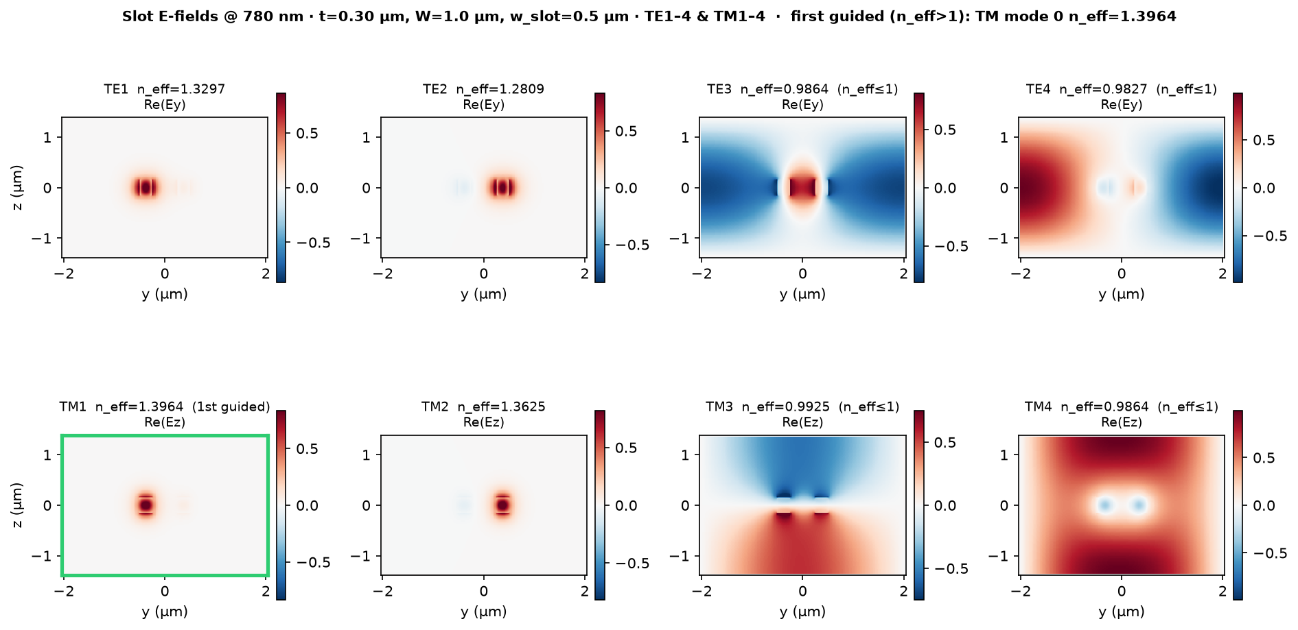
Artifacts
runs/slot_waveguide_modes_2d_t300nm_W1p0_slot0p5_780nm/summary.jsonfigures/slot_waveguide_Efields_TE1-4_TM1-4_t300nm_W1p0_slot0p5_780nm.png
Wide-gap air-mode check — t = 300 nm, W = 1.5 µm, slot = 1.0 µm @ 780 nm
Question
Can two Si₃N₄ rails support a guided mode mostly in a 1 µm air gap, and in particular are the next higher modes (TE3/TE4/TM3/TM4) guided air modes?
Geometry and numerical check
Plain, unpatterned slot cross-section (no fishbone), air cladding:
| Parameter | Value |
|---|---|
| wavelength | 780 nm |
| Si₃N₄ index | 2.00 (constant model) |
| rail thickness | 0.30 µm |
| total rail-to-rail outer width W | 1.50 µm |
| air gap | 1.00 µm |
| individual rail width | 0.25 µm |
| primary solver domain (y × z) | 7.5 × 5.3 µm² |
| confirmation domain (y × z) | 9.5 × 6.3 µm² |
| boundary | PML in y and z |
The primary domain leaves 3.0 µm air beyond each outer rail in y and 2.5 µm
above/below the film. It is deliberately much wider than the guide. Tidy3D's
local ModeSolver was asked for 24 modes. A mode is treated as bound only when
n_eff > 1 and its field decays at the mode-plane boundary. The final two
columns are sampled electric-field-intensity fractions: in the 1 µm gap, and
in the outermost 10% of the computational window, respectively.
| Family | order | n_eff (wide) | n_eff (confirmation) | gap | outer 10% | classification |
|---|---|---|---|---|---|---|
| TE | 1 | 1.2834 | 1.2949 | 17.7% | ~0% | bound, rail-dominated |
| TE | 2 | 1.2832 | 1.2946 | 17.9% | ~0% | bound, rail-dominated |
| TM | 1 | 1.3443 | 1.3625 | 6.8% | ~0% | bound, rail-dominated |
| TM | 2 | 1.3441 | 1.3624 | 6.5% | ~0% | bound, rail-dominated |
| TE | 3 | 0.9959 | 0.9973 | 1.4% | 19.0% | radiation / box state |
| TE | 4 | 0.9956 | 0.9971 | 2.1% | 21.0% | radiation / box state |
| TM | 3 | 0.9968 | 0.9981 | 18.6% | 15.7% | radiation / box state |
| TM | 4 | 0.9967 | 0.9977 | 23.2% | 15.3% | radiation / box state |
The solver explicitly reported non-decay at the boundary for modes starting at mode index 4 (which contains TM3 and the corresponding higher-order states). Increasing the domain shifts these near-light-line values toward 1 and leaves a large outer-window intensity fraction: the expected signature of the air continuum, not a guided mode. By contrast, the four bound rail modes have negligible outer-window intensity.
Conclusion
For an ordinary two-rail Si₃N₄/air slot guide, this requested 1 µm gap does not produce a bound, gap-dominant air mode. The slot effect remains visible in the guided TE pair, but only about 18% of sampled electric intensity is in the gap; TM is even less gap-localized. The apparently air-like TM3/TM4 states are not guided.
More generally, a conventional index-guided mode in an all-air cladding must
remain above the air light line (n_eff > 1). A very wide low-index gap loses
the evanescent overlap that makes a slot mode work. A truly air-localized guided
mode therefore needs an additional confinement mechanism, e.g. a 2D photonic
bandgap / hollow-core design, antiresonant guidance, or a periodic structure
that opens a stop band around the air defect. The fishbone's eventual periodic
design could be explored for this purpose; the plain slot alone cannot provide
it here.
Artifacts
| File | Role |
|---|---|
runs/slot_waveguide_modes_2d_t300nm_W1p5_slot1p0_wide_780nm/summary.json |
24-mode wide-domain spectrum and localization metrics |
runs/slot_waveguide_modes_2d_t300nm_W1p5_slot1p0_xwide_780nm/summary.json |
larger-domain confirmation spectrum |
figures/slot_waveguide_cross_section_2d_t300nm_W1p5_slot1p0_wide_780nm.png |
cross-section |
figures/slot_waveguide_modes_2d_t300nm_W1p5_slot1p0_wide_780nm.png |
TE1–TE4 and TM1–TM4 field panels |
Regenerate:
.venv/bin/python engines/atom_fishbone_coupler/package/atom_fishbone/slot_waveguide_modes_2d.py \
  --W 1.5 --slot 1.0 --thickness 0.3 --pad-y 3.0 --pad-z 2.5 \
  --num-modes 24 --per-pol 4 --tag t300nm_W1p5_slot1p0_wide_780nm
Interrupted Si₃N₄ slab — 0.5 µm air gap, t = 300 nm @ 780 nm
Geometry
Two Si₃N₄ slabs, each extending arbitrarily far in ±y, are separated by a 0.5 µm-wide air gap. The film is 0.30 µm thick, air-clad above and below.
This is materially different from a finite-width slot guide: in the infinite-width limit each side is a laterally unbounded slab waveguide. To check the limit numerically, I used a wide finite proxy with two 2.0 µm wide Si₃N₄ regions (W = 4.5 µm including the gap), with 3.0 µm lateral air padding on both exterior sides and 2.5 µm above/below the film.
Result
It does not support a discrete, air-guided gap mode.
The six highest-n_eff modes of each polarization are conventional slab modes:
| Family | n_eff range (first 4) | gap electric-intensity fraction |
|---|---|---|
| TE-like | 1.6965 → 1.6182 | 0.48% → 1.26% |
| TM-like | 1.6251 → 1.5939 | 0.04% → 0.20% |
All have negligible field at the exterior computational boundary, so they are vertically guided slab modes. Their field is overwhelmingly in the Si₃N₄, not the gap. No computed bound state is localized to the 0.5 µm air defect.
Why the infinite-width limit rules it out
The air gap is a lower-index interruption inside the high-index slab. It is a lateral anti-guide: a wave can lower its effective index barrier by spreading indefinitely into either Si₃N₄ half-slab. Thus the finite-proxy slab modes become a continuous set parameterized by lateral wavevector as rail width goes to infinity; none becomes a normalizable gap-localized eigenmode.
The familiar slot enhancement can raise the normal electric field in a low-index gap between finite rails, but it does not turn a low-index trench in an unbounded high-index slab into a bound air-core waveguide. To make this geometry air-guiding, add lateral reflection/confinement, for example a 2D photonic bandgap surrounding the gap, an antiresonant reflector, or finite width rails.
Artifact
runs/slot_waveguide_modes_2d_t300nm_W4p5_slot0p5_wide_slab_780nm/summary.json
Stage 2 — 3D MPB fishbone unit cell, first band-edge baseline
Requested physical geometry
| Parameter | Value |
|---|---|
period a |
0.23 µm |
Si₃N₄ thickness t |
0.30 µm (carried forward from the preceding stage) |
rail outer-to-outer width W |
1.20 µm |
continuous air slot w_slot |
1.00 µm |
rail width (W − w_slot)/2 |
0.10 µm |
fishbone amplitude A |
0.50 µm |
| tooth length along x | a/2 = 0.115 µm |
| core index model | n_Si3N4 = 2.00, hence ε = 4.0 |
| cladding | air (ε = 1) |
MPB construction and unit handling
MPB uses dimensionless units with a = 1. The driver therefore divides
every physical length by 0.23 µm before creating geometry:
| Quantity | MPB units |
|---|---|
| x period | 1.0000 |
t |
1.30435 |
W |
5.21739 |
| slot | 4.34783 |
| rail width | 0.43478 |
A |
2.17391 |
| tooth length | 0.50000 |
The isolated guide is represented by an air supercell of size
1 × 18.2609 × 10.0000 (x, y, z), i.e. 1.0 µm air padding on each exterior
y and z side. The rails are separate full-period blocks. Each tooth occupies
the y interval [W/2, W/2 + A] (or its negative mirror), while the rail ends
at ±W/2; they touch only on a face and have zero overlapping volume.
This matters because MPB does not require, or benefit from, overlapping
dielectrics to make a connected shape.
First completed 3D MPB result — targeted Γ–X band edge
MPB was newly installed for this stage. A complete first-pass run used:
| Solver setting | Value |
|---|---|
| spatial resolution | 8 pixels / a (grid 8 × 147 × 80) |
| mesh size | 5 |
| eigensolver residual | 1e-4 |
| target frequency | a/λ = 0.30 |
| computed branch | one full-vector 3D eigenbranch nearest target |
| k path | Γ (0,0,0) → X (0.5,0,0) |
| k point | a/λ |
equivalent wavelength for a = 230 nm |
|---|---|---|
| Γ | 0.293477 | 783.7 nm |
| X | 0.322780 | 712.6 nm |
The selected branch therefore rises by 0.029303 a/λ from Γ to X. The
result is plotted below.
Interpretation and limitation
This establishes that the exact non-overlapping 3D geometry runs in MPB and places a target-near branch around the 780 nm design neighborhood at Γ. It is not yet a converged full band diagram or a photonic bandgap claim: the first pass traces one target-selected branch at only the two band edges, with a coarse spatial resolution. In this large air supercell, an untargeted multi-band solve is dominated by nearly-degenerate air-box states; it should next be split into mirror-symmetry sectors and converged in resolution, supercell padding, k-point density, and number of branches before interpreting guided-band gaps or radiation loss.
Artifacts
| File | Role |
|---|---|
package/atom_fishbone/fishbone_band_3d.ctl |
reproducible MPB unit-cell construction and Γ–X solve |
package/atom_fishbone/plot_fishbone_band_3d.py |
parses MPB frequencies and plots bands |
runs/fishbone_band_3d_W1p2_gap1p0_A0p5_a0p23_r8_target0p30_GammaX/mpb_stdout.txt |
raw MPB log |
runs/fishbone_band_3d_W1p2_gap1p0_A0p5_a0p23_r8_target0p30_GammaX/mpb_stdout.csv |
Γ/X frequency data |
runs/fishbone_band_3d_W1p2_gap1p0_A0p5_a0p23_r8_target0p30_GammaX/fishbone_band_3d-epsilon.h5 |
3D dielectric grid |
figures/fishbone_band_3d_W1p2_gap1p0_A0p5_a0p23_r8_target0p30_GammaX.png |
plotted result |
Regenerate:
RUN=engines/atom_fishbone_coupler/runs/fishbone_band_3d_W1p2_gap1p0_A0p5_a0p23_r8_target0p30_GammaX
mkdir -p "$RUN"
(cd "$RUN" && mpb ../../package/atom_fishbone/fishbone_band_3d.ctl > mpb_stdout.txt)
.venv/bin/python engines/atom_fishbone_coupler/package/atom_fishbone/plot_fishbone_band_3d.py \
  "$RUN/mpb_stdout.txt" \
  engines/atom_fishbone_coupler/figures/fishbone_band_3d_W1p2_gap1p0_A0p5_a0p23_r8_target0p30_GammaX.png
Stage 2 update — MPB band-edge axis in π/a units
The band-diagram x-axis now uses k_x/(π/a), appropriate for the 1D Bloch
path. The displayed edge segment is 0.75 π/a to 1.00 π/a (X), which MPB
expresses as k_x = 0.375 to 0.5 in its native 2π/a units.
k_x/(π/a) |
MPB k_x |
a/λ |
λ for a = 230 nm |
|---|---|---|---|
| 0.75 | 0.375 | 0.302415 | 760.5 nm |
| 1.00 (X) | 0.500 | 0.322687 | 712.9 nm |
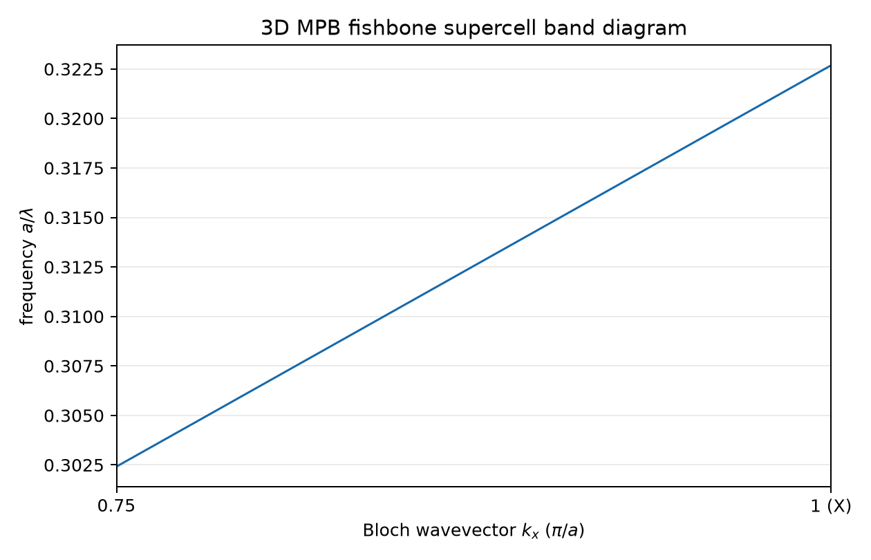
Only one line is shown because this preliminary MPB calculation deliberately
targeted one full-vector eigenbranch near a/λ = 0.30; it was not a
multi-band calculation. The next full diagram must use symmetry-sector
filtering / guided-mode identification to avoid the large air-supercell's
near-degenerate radiation-box bands.
Artifacts:
runs/fishbone_band_3d_W1p2_gap1p0_A0p5_a0p23_r8_target0p30_edge/figures/fishbone_band_3d_W1p2_gap1p0_A0p5_a0p23_r8_target0p30_edge.png
SiO₂/air slot waveguide — 1.0 µm gap @ 780 nm
Aim and chosen geometry
This is a finite, air-clad SiO₂ slot waveguide without fishbone teeth. To give the 1.0 µm gap a favorable test, each rail is 1.0 µm wide and the film is 0.50 µm thick. The wide rails avoid simple rail cutoff; the 3.0 µm lateral and 2.5 µm vertical air padding make the outer boundaries non-participating.
| Parameter | Value |
|---|---|
| λ | 780 nm |
| core | SiO₂, n = 1.45 (constant model) |
t |
0.50 µm |
total width W |
3.00 µm |
| air slot | 1.00 µm |
| rail width | 1.00 µm each |
| domain, y × z | 9.0 × 5.5 µm² |
| solver | local Tidy3D ModeSolver, 20 modes |
Results
All eight shown modes lie above the air light line and decay at the outer boundaries, so they are guided. However, their electric intensity is localized in the oxide rails, not in the 1 µm air gap.
| Label | mode | n_eff | gap electric-intensity fraction | classification |
|---|---|---|---|---|
| TE1 | 0 | 1.3081 | 1.5% | guided, rail-dominated |
| TE2 | 1 | 1.3074 | 1.8% | guided, rail-dominated |
| TE3 | 4 | 1.1748 | 7.0% | guided, rail-dominated |
| TE4 | 5 | 1.1726 | 8.2% | guided, rail-dominated |
| TM1 | 2 | 1.2762 | 1.0% | guided, rail-dominated |
| TM2 | 3 | 1.2752 | 1.0% | guided, rail-dominated |
| TM3 | 6 | 1.1648 | 4.4% | guided, rail-dominated |
| TM4 | 7 | 1.1607 | 4.6% | guided, rail-dominated |
Conclusion
The 1 µm SiO₂ slot is a conventional finite-rail waveguide, not an air-core guide. Lower core contrast makes the modes broader, but it does not create a mode that lives primarily in the gap. Of the tested modes, TE4 puts the most sampled electric intensity in the gap (8.2%)—still far from air dominated.
Artifacts
| File | Role |
|---|---|
runs/slot_waveguide_modes_2d_sio2_t500nm_W3p0_slot1p0_wide_780nm/summary.json |
20-mode spectrum and localization metrics |
figures/slot_waveguide_cross_section_2d_sio2_t500nm_W3p0_slot1p0_wide_780nm.png |
SiO₂/air cross-section |
figures/slot_waveguide_modes_2d_sio2_t500nm_W3p0_slot1p0_wide_780nm.png |
TE1–4 and TM1–4 fields/intensities |
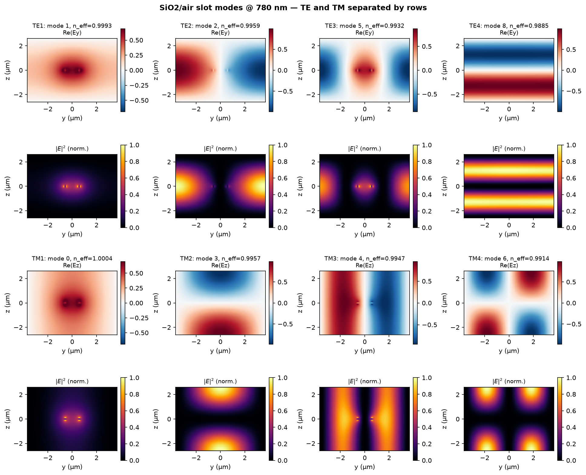
SiO₂/air slot waveguide — tiny 0.15 × 0.15 µm rails, 1.0 µm gap @ 780 nm
Geometry
Requested geometry: two SiO₂ rails, each 0.15 µm wide × 0.15 µm thick,
separated by a 1.0 µm air gap. Thus W = 1.30 µm. The computation used the
same generous 3.0 µm lateral and 2.5 µm vertical air padding as the other wide
domain tests.
Results
| Label | mode | n_eff | gap electric-intensity fraction | interpretation |
|---|---|---|---|---|
| TE1 | 1 | 0.99927 | 28.8% | below air light line; radiation-box state |
| TE2 | 2 | 0.99592 | 1.1% | radiation-box state |
| TE3 | 5 | 0.99316 | 14.8% | radiation-box state |
| TE4 | 8 | 0.98847 | 13.8% | radiation-box state |
| TM1 | 0 | 1.00036 | 31.5% | marginally bound / near-cutoff |
| TM2 | 3 | 0.99571 | 26.4% | radiation-box state |
| TM3 | 4 | 0.99467 | 2.4% | radiation-box state |
| TM4 | 6 | 0.99139 | 1.8% | radiation-box state |
Only TM1 sits infinitesimally above the air light line, and even it has 5.6% of sampled electric intensity in the outermost 10% of the domain. It should be treated as near-cutoff rather than a robust guided air mode. The other modes' tempting gap fractions arise because they are extended air-continuum states; the field plots visibly reach the computational boundary.
TE and TM on separate rows
For readability, the plot puts TE field/intensity rows first and TM field/intensity rows second.
Conclusion
Making the SiO₂ rails tiny does not create the desired 1 µm air-gap guide. It
removes robust index guidance instead: all TE modes and all but one TM mode are
below n_eff = 1; the remaining TM1 is only 0.00036 above cutoff. This is not
a usable air-guided mode.
Artifacts
| File | Role |
|---|---|
runs/slot_waveguide_modes_2d_sio2_t150nm_rails150nm_slot1p0_wide_780nm/summary.json |
20-mode spectrum and localization metrics |
figures/slot_waveguide_cross_section_2d_sio2_t150nm_rails150nm_slot1p0_wide_780nm.png |
tiny-rail cross-section |
figures/slot_waveguide_TE_TM_rows_2d_sio2_t150nm_rails150nm_slot1p0_wide_780nm.png |
requested TE/TM row-separated field view |