Gen 3 — facet-cleave stamp coupling with silver-mirror Stark tuning
Active build. Full architecture, wafer stack, and molecule-site geometry
below; source of truth is device_architectures/v3/README.md in the repo.
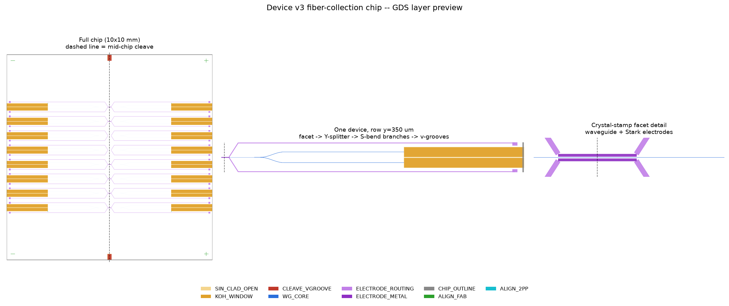
Chip GDS layout: full 10x10 mm die (8 waveguide rows, mirror-symmetric about the mid-chip cleave), one device's facet-to-v-groove path, and the crystal-stamp facet detail (waveguide + Stark electrodes).
Goal
A 10 mm silicon chip carrying 5-10 parallel Si3N4/SiO2 waveguides (this build: 8, on a 700 um pitch). The chip is cleaved down the middle to expose an optically flat waveguide facet; a hexagonal (~50 um) DBT-doped anthracene crystal is stamped onto that facet. A free-space laser focused through an NA=0.6 objective excites the molecule from above; emission couples into the Si3N4 waveguide, passes through a 50:50 splitter into two arms, and each arm couples to a fiber seated in a KOH-etched v-groove via a 2PP-printed aspheric lens pair. In the silver-mirror variant, the second cleaved half gets a 50 nm Ag coating and is re-fused against the crystal, forming a molecule-in-a-cavity geometry with in-plane Stark-tuning electrodes.
Wafer stack
525 um Si / 4 um SiO2 undercladding / 300 nm Si3N4 core film. KOH etch windows must open through the Si3N4 + SiO2 mask down to bare Si before the v-groove wet etch (54.74 deg <111> sidewalls).
Pieces and results so far
- Chip + wafer GDS, and fiber-coupling lens design — waveguides, Y-junction splitters, KOH windows, cleave-guide v-grooves, Stark electrodes + routing, two alignment-mark systems (fab + 2PP), a 60-die 4-inch wafer layout; plus the ray-traced two-lens 2PP relay (waveguide facet -> fiber) with STL export.
- 50:50 splitter FDTD (same page,
splitter_fdtd/subfolder) — Y-junction: 49.97%/50.03% balanced split, 2.37 dB excess loss (flagged for a longer-bend follow-up iteration). - Facet-mirror emitter coupling (tidy3d) — collection efficiency 50.5%, excitation efficiency 52.0% (vs. ideal free-space NA=0.6 focus), cross-talk 2.6%. Idealized (translationally broad crystal/mirror) upper-bound estimate — see caveats on that page.
- Stark-tuning electrostatics — dEy/dV = -2.08e4 V/m per volt at the molecule; anthracene's DC dielectric constant is an unverified placeholder (flagged on that page).
Open questions across workstreams
Every sub-project above independently flagged its own assumptions; the recurring cross-cutting ones are: (1) the exact z-stack interpretation where the silver mirror bonds to the crystal (each workstream made the same reasonable reading independently, but it's still an interpretation, not a literal spec transcription); (2) waveguide width (0.4 um) and Stark electrode gap (2 um) are consistent across all workstreams but not yet pinned by a real GDS-to-simulation round trip; (3) the fiber-facing waveguide facet is assumed to be a separate smooth etch, not the sloped KOH wall itself.