Anthracene slab ↔ waveguide coupling
Can a Si3N4 waveguide exchange energy with a dipole via the crystal slab mode when it terminates short of the emitter?
Investigate whether a Si3N4 waveguide under an anthracene crystal slab can exchange energy with a dipole (emitter) at the crystal center when the guide terminates short of the center — coupling via the crystal slab mode.
Question
Can a waveguide excite a crystal mode that propagates to a central dipole? Equivalently (reciprocity): can a central dipole couple into that waveguide through the slab mode?
Geometry (sim 01)
| Layer | Spec |
|---|---|
| Anthracene slab | n = 1.8, 200 nm thick, infinite in x,y |
| Si3N4 waveguide | 400 nm wide × 300 nm thick, under the crystal, touching |
| Gap | WG tip ends 2 µm before the dipole (x = 0) |
| Background | air |
| Wavelength | 780 nm (DBT:anthracene line) |
Run
Requires Tidy3D credentials (tidy3d ≥ 2.x) and FlexCredits.
Outputs
reports/sim01_dipole_to_wg.md/.html— full reportdata/sim01_dipole_to_wg_metrics.jsondata/simulations/sim01_dipole_to_wg_{Ex,Ey,Ez}.hdf5figures/sim01_*
Layout
config.py                 study parameters
simulation.py             Tidy3D geometry / monitors
run_sim01_dipole_to_wg.py run + analyze + report
reporting.py              md/html helpers
Results
Sim 01 — Dipole in anthracene slab → Si3N4 waveguide coupling
First simulation in the anthracene slab / waveguide coupling investigation. A point dipole sits at the center of a 200 nm anthracene crystal (n = 1.8, laterally infinite). A Si3N4 strip waveguide (400 nm × 300 nm, n = 2.0) lies under the crystal, touching its bottom face, but terminates a few microns before the dipole. We measure how much of the dipole's radiated power couples into guided modes of the strip — related by reciprocity to waveguide excitation of crystal modes that reach the center.
Physical question
Can a waveguide excite a mode of the anthracene crystal that reaches a dipole at the center? Equivalently (reciprocity): can a dipole at the crystal center launch power into a waveguide that stops short of the emitter, via the crystal slab mode as an intermediary?
This simulation answers the second form with a quantitative coupling efficiency η = P_guided / P_total.
Geometry
| Parameter | Value |
|---|---|
| Anthracene index | n = 1.8 |
| Anthracene thickness | 200 nm |
| Anthracene lateral extent | infinite (x, y) |
| Si3N4 index | n = 2.0 |
| Waveguide cross-section (W × H) | 400 × 300 nm |
| Waveguide tip position | x = -2.00 µm |
| Gap (tip → dipole) | 2.00 µm |
| Mode monitor x | -3.50 µm |
| Dipole position | (0, 0, 100 nm) crystal mid-plane |
| Background | air |
| Emitter wavelength | 780 nm |
| Analysis band | 720–860 nm (15 pts) |
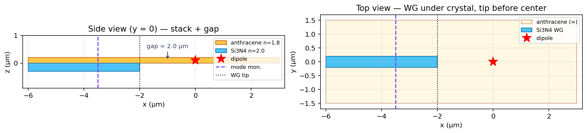
Geometry: side view (XZ) and top view (XY)
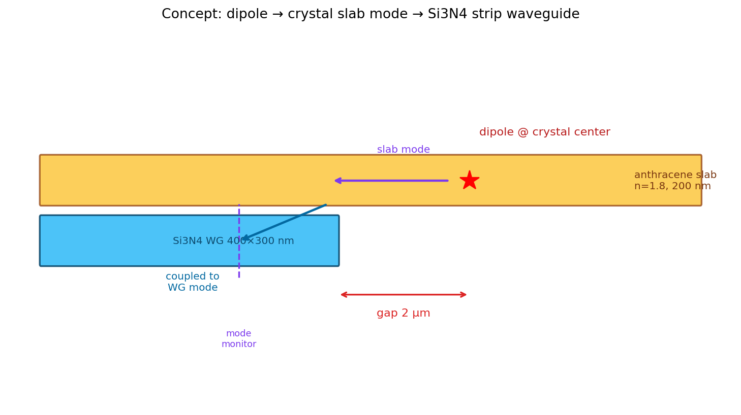
Concept schematic: dipole → slab mode → waveguide
Stack (z vertical)
  z = 200 nm  ─ top of anthracene
  z = 100 nm   ★ dipole (crystal mid-plane)
  z = 0             ─ crystal / WG interface (touching)
  z = -300 nm ─ bottom of Si3N4 waveguide
The waveguide occupies x ∈ [domain left, −gap] and does not extend under the dipole. Between the tip and the dipole there is only the anthracene slab (plus air cladding), so any power that reaches the strip must travel as a crystal slab mode (or free-space radiation that later couples).
Method
- Solver: Tidy3D FDTD (cloud)
- Source:
PointDipolewith broadband Gaussian pulse; polarizations Ex, Ey, Ez - Total power: closed six-face field-monitor box around the dipole
- Guided power:
ModeMonitoron a WG cross-section inset from the tip (1.5 µm into the guide); direction −x (into the guide) - Guided-mode filter: |Im(n_eff)| < 0.01 and Re(n_eff) > 1.05 (leaky / continuum modes excluded from η_guided)
- Also report: mode-0 only, |FluxMonitor| / P_total, and unfiltered mode sum
- Symmetry: y-mirror only (structure is one-sided in x)
- Mesh: auto, min 18 steps/λ, refined near WG and dipole
- Run time: 2.0 ps, shutoff 1e-05 (solver early-exited ~2% of run time once field energy decayed)
Results @ 780 nm
| Pol | η guided | η mode0 | η |flux| | η all modes* | n_eff (best guided) | P_total | | --- | --- | --- | --- | --- | --- | --- | | Ex | 0.321% | 0.022% | 0.475% | 0.770% | 1.4784 | 4.176e+03 | | Ey | 10.789% | 5.259% | 12.505% | 20.820% | 1.4777 | 4.172e+03 | | Ez | 2.721% | 2.704% | 6.589% | 3.244% | 1.6720 | 2.760e+03 |
* all modes includes leaky ModeMonitor solutions and can overestimate true guided power — prefer η guided / η mode0 / η |flux|.
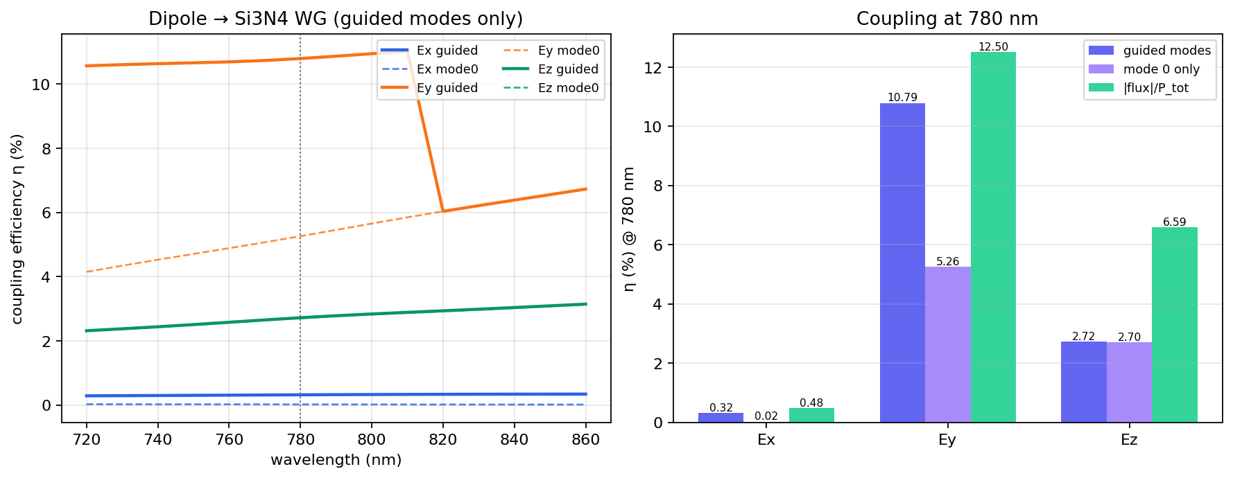
Guided coupling spectrum and bar chart @ 780 nm
Mode decomposition @ 780 nm
| Pol | mode | class | n_eff (re) | n_eff (im) | P (−x) | η contrib |
|---|---|---|---|---|---|---|
| Ex | 0 | guided | 1.6720 | 3.41e-08 | 9.144e-01 | 0.022% |
| Ex | 1 | guided | 1.4784 | 4.81e-03 | 1.248e+01 | 0.299% |
| Ex | 2 | leaky | 1.4484 | 5.10e-02 | 1.078e+01 | 0.258% |
| Ex | 3 | leaky | 1.3943 | 1.72e-01 | 8.000e+00 | 0.192% |
| Ey | 0 | guided | 1.6722 | -1.08e-06 | 2.194e+02 | 5.259% |
| Ey | 1 | guided | 1.4777 | 8.66e-03 | 2.307e+02 | 5.530% |
| Ey | 2 | leaky | 1.4217 | 7.88e-02 | 2.330e+02 | 5.585% |
| Ey | 3 | leaky | 1.3711 | 6.35e-02 | 1.855e+02 | 4.446% |
| Ez | 0 | guided | 1.6720 | 3.41e-08 | 7.463e+01 | 2.704% |
| Ez | 1 | guided | 1.4784 | 4.81e-03 | 4.503e-01 | 0.016% |
| Ez | 2 | leaky | 1.4484 | 5.10e-02 | 4.443e+00 | 0.161% |
| Ez | 3 | leaky | 1.3943 | 1.72e-01 | 1.001e+01 | 0.363% |
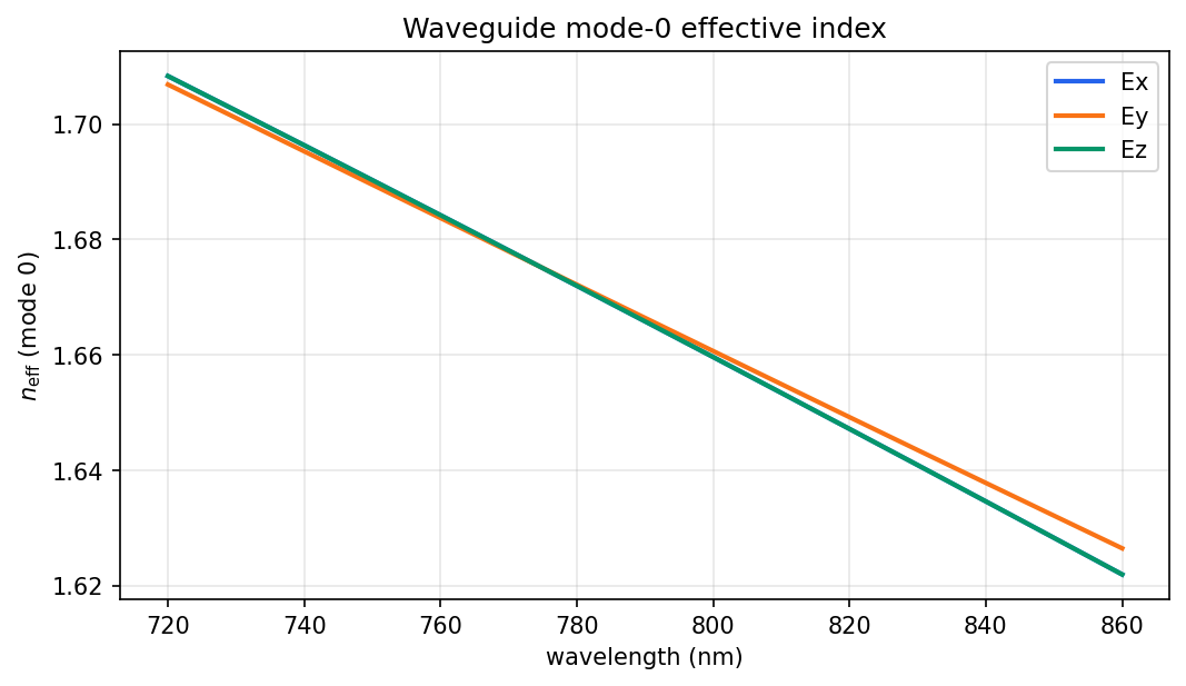
Effective index of mode 0 vs wavelength
Electric field @ 780 nm
Polarization Ex
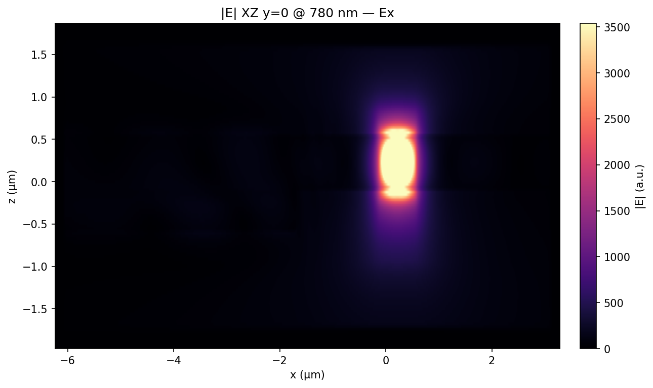
|E| in XZ plane (y=0) — Ex
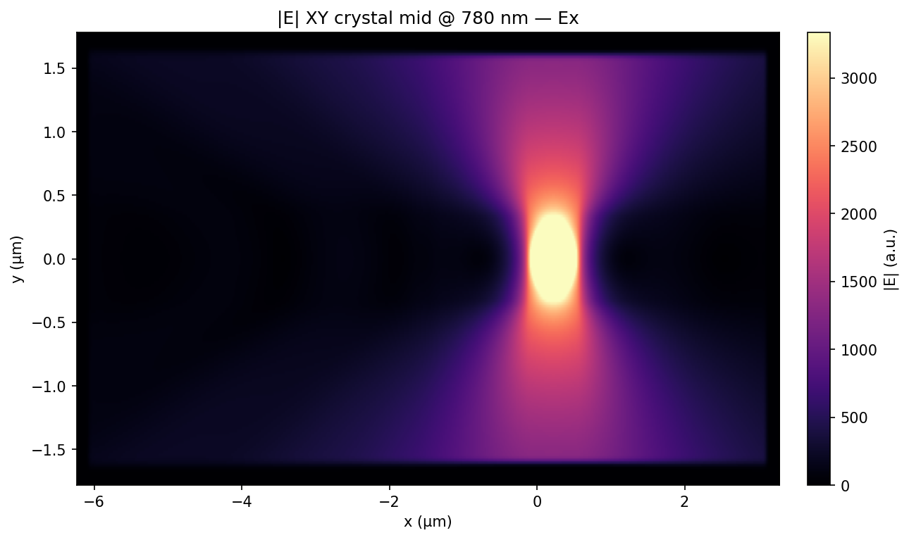
|E| in XY at crystal mid-plane — Ex
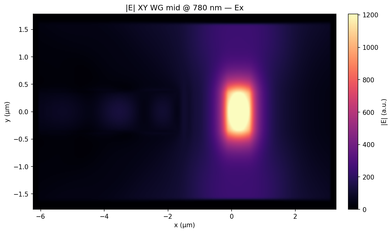
|E| in XY at WG mid-height — Ex
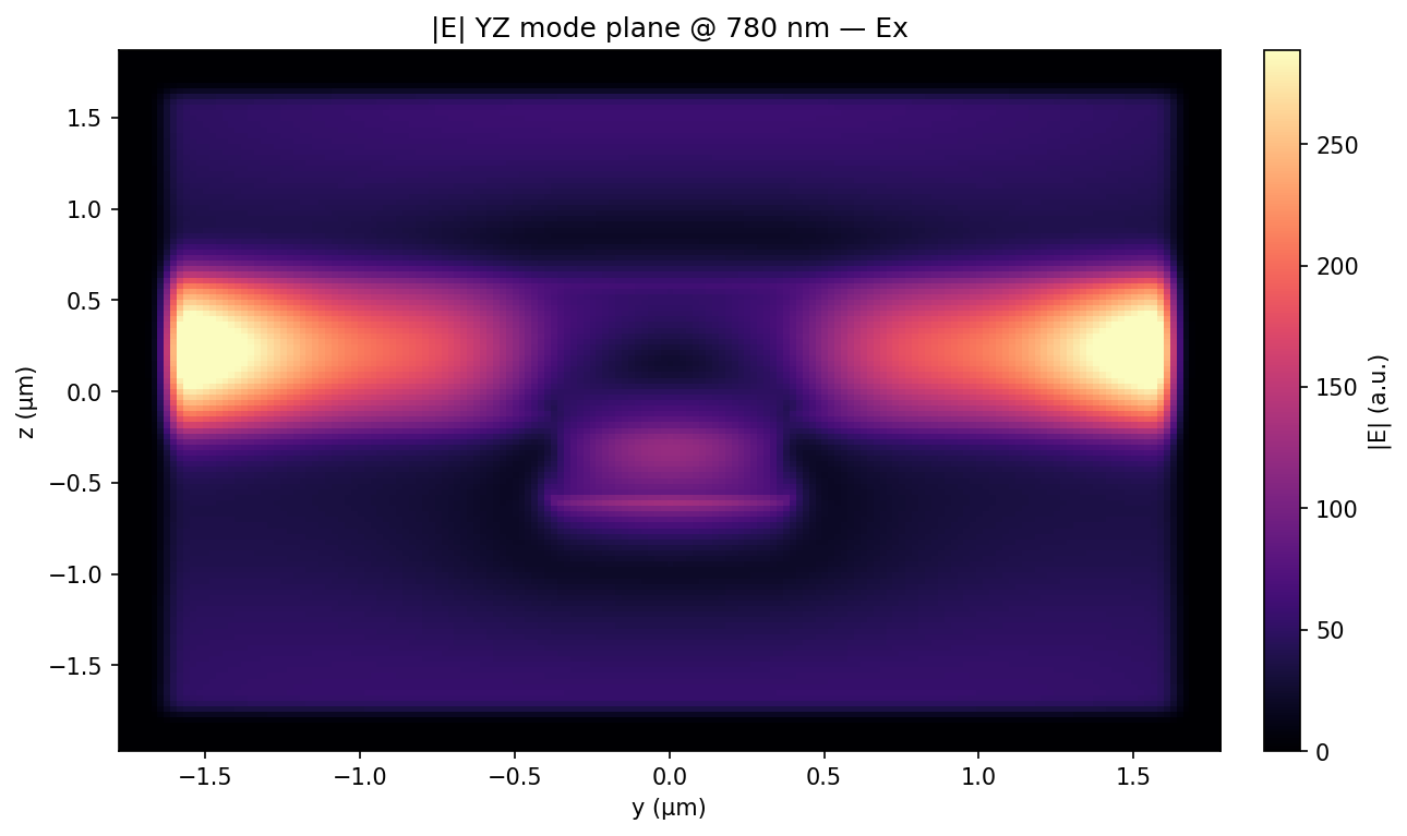
|E| in YZ at mode monitor — Ex
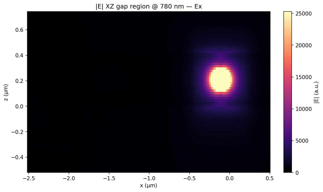
|E| in XZ across the gap — Ex
Polarization Ey
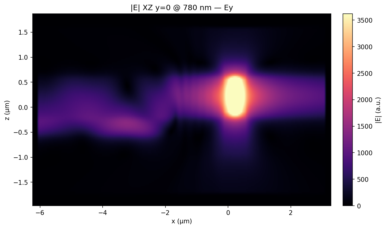
|E| in XZ plane (y=0) — Ey
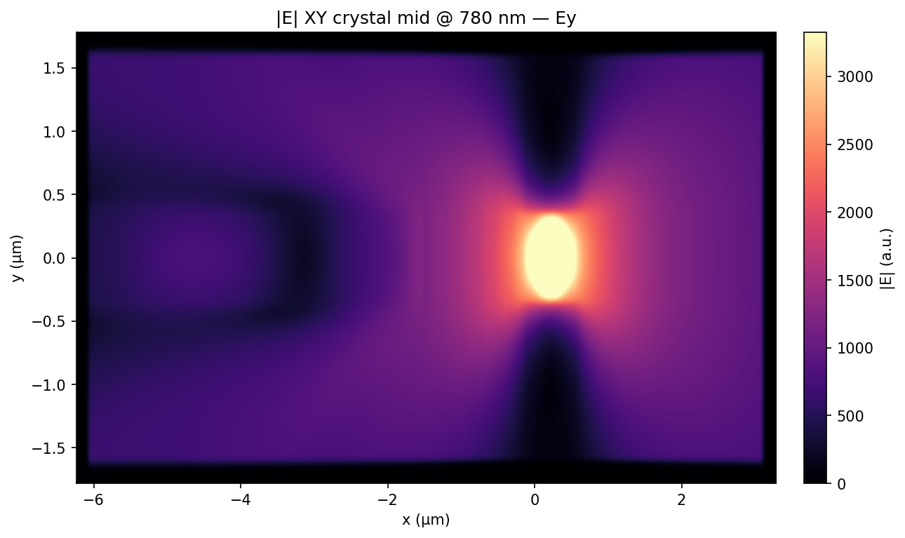
|E| in XY at crystal mid-plane — Ey
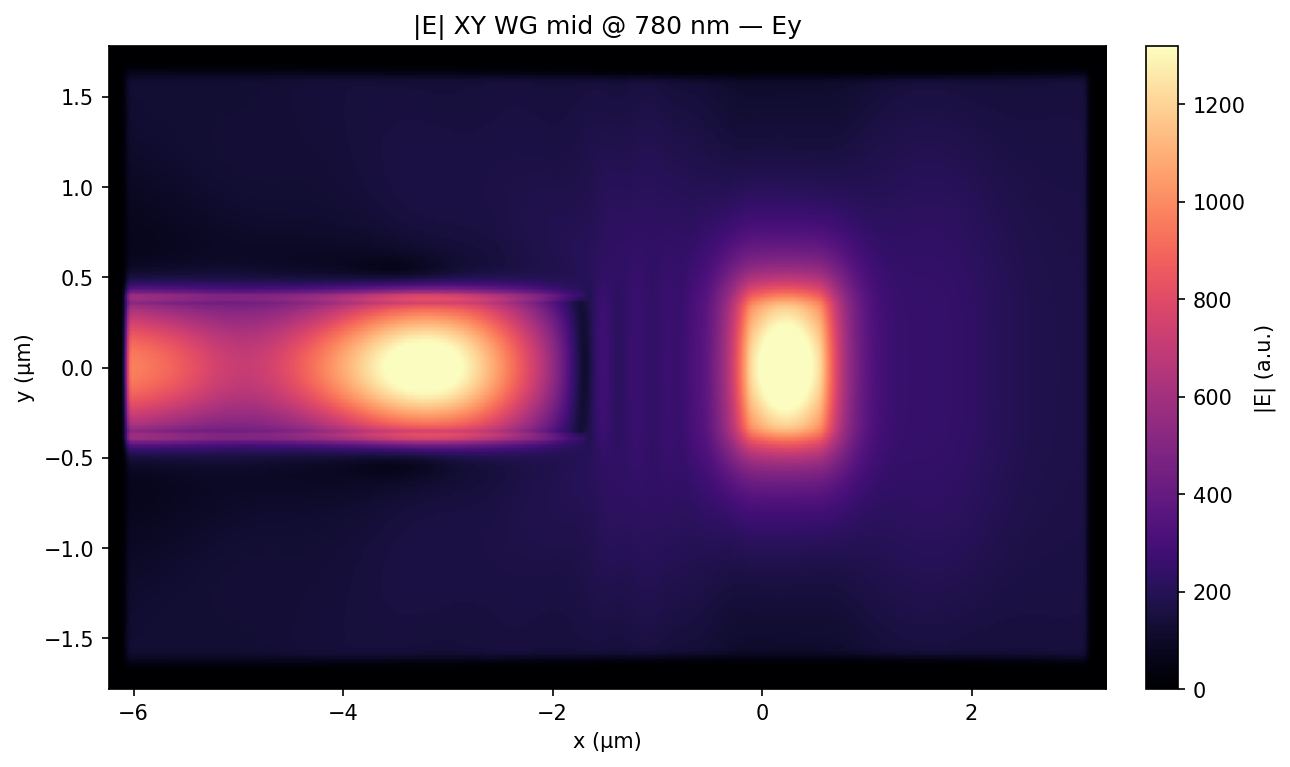
|E| in XY at WG mid-height — Ey
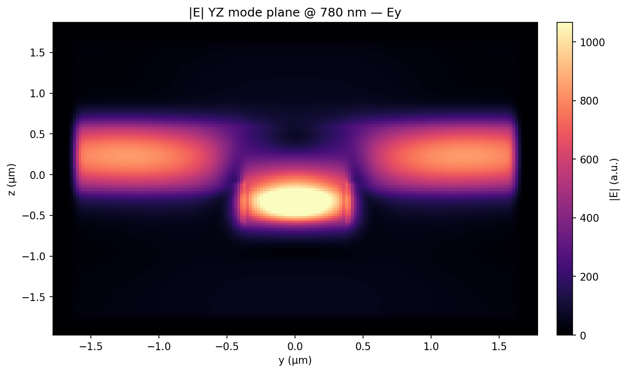
|E| in YZ at mode monitor — Ey
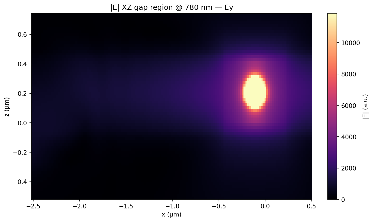
|E| in XZ across the gap — Ey
Polarization Ez
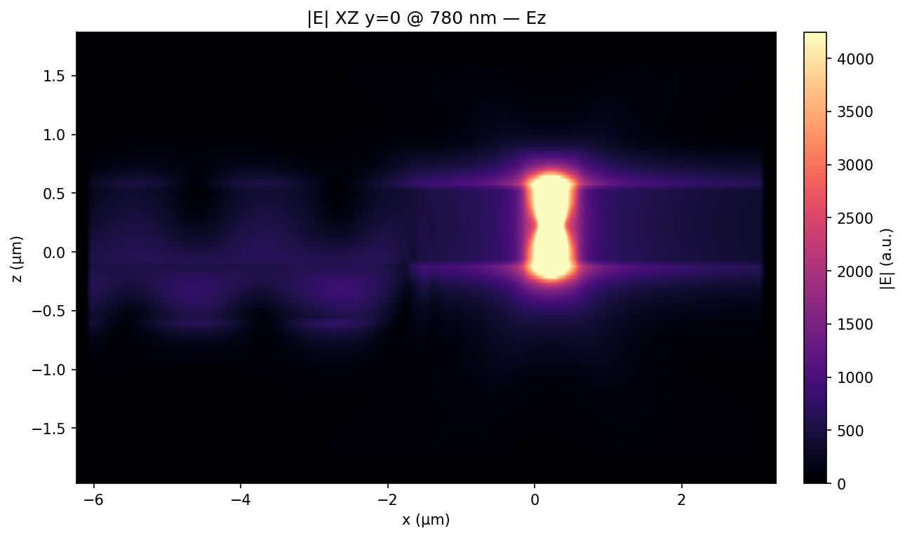
|E| in XZ plane (y=0) — Ez
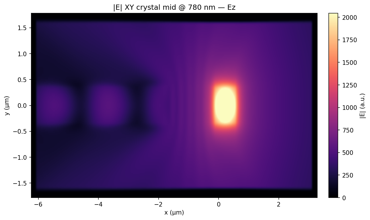
|E| in XY at crystal mid-plane — Ez
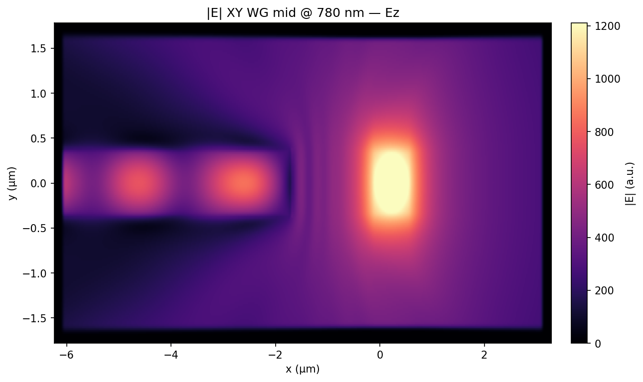
|E| in XY at WG mid-height — Ez
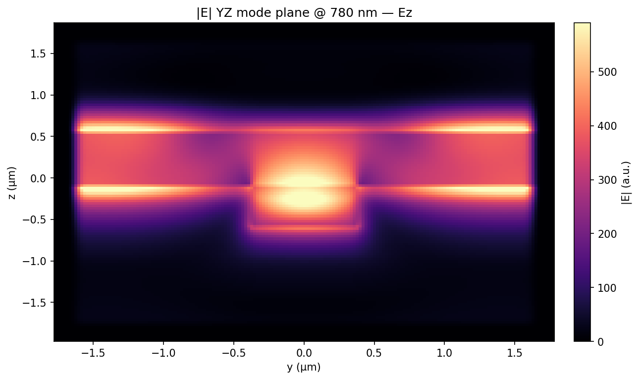
|E| in YZ at mode monitor — Ez
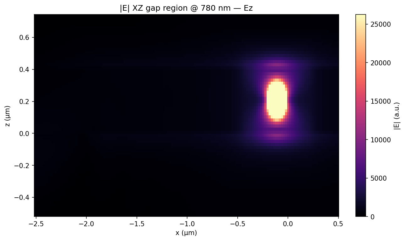
|E| in XZ across the gap — Ez
Interpretation
- Best polarization for true guided coupling: Ey with η_guided ≈ 10.79% at 780 nm (mode-0: 5.26%; |flux|/P: 12.50%).
- Gap between waveguide tip and dipole: 2.0 µm. Power crosses this gap in the anthracene slab (and/or free space) before overlapping the Si3N4 strip.
- Ey (in-plane, transverse to the strip) couples most strongly — expected for TE-like strip modes under a high-index slab.
- Ez (vertical) couples moderately into the TM-like fundamental (η_guided ≈ 2.72%).
- Ex (along the guide) couples weakly to guided modes (η_guided ≈ 0.32%).
- Field maps show the dipole field extending through the gap and field intensity continuing into the Si3N4 region (x < −2 µm), consistent with slab-mediated transfer.
- Absolute efficiencies are a baseline for an untapered abrupt tip under a weakly confined crystal slab — not an optimized coupler.
- By reciprocity, the same η is the fraction of power a waveguide mode launched toward the tip would deliver into the corresponding dipole channel (with consistent normalization).
Answer: can a waveguide excite a crystal mode that reaches the dipole?
Yes. Coupling is nonzero for all three polarizations, and for Ey the guided-mode channel is at the few-percent level even with a 2 µm gap and no tip engineering. A waveguide can feed energy into crystal modes that reach the center; whether that is enough for an application depends on gap, tip design, polarization, and collection optics — topics for follow-up sims.
Simulation cost
| Polarization | FlexCredits | task_id |
|---|---|---|
| Ex | 0.0250 | fdve-47af1ac5-54b8-4e24-abb9-d64cb4aa1d21 |
| Ey | 0.0250 | fdve-5029bfe0-304c-4985-b0da-483cef27eb1b |
| Ez | 0.0250 | fdve-088cb934-dadb-4fbf-bfdc-10e55b851dcb |
| Total | 0.0750 |
Files
- Metrics JSON:
data/sim01_dipole_to_wg_metrics.json - Simulation data:
data/simulations/sim01_dipole_to_wg_{Ex,Ey,Ez}.hdf5 - Figures:
figures/sim01_* - This report:
reports/sim01_dipole_to_wg.md/.html
Next steps (suggested)
- Sweep gap (0.5–5 µm) to map slab-mode propagation / coupling length.
- Reverse excitation: ModeSource in the WG → field / power at the dipole.
- Tip engineering: adiabatic taper, grating, or resonator under the crystal.
- Substrate: SiO2 under the WG (more realistic chip stack).
- Crystal-only reference (no WG) for radiated-power baseline.
Downloads
FDTD simulation study only -- no GDS/STL deliverable files exist in this tree.
Source: nanophotonic_devices/emitter_coupling/anthracene_slab_wg_coupling_v1/