Single-molecule device v1 (master)
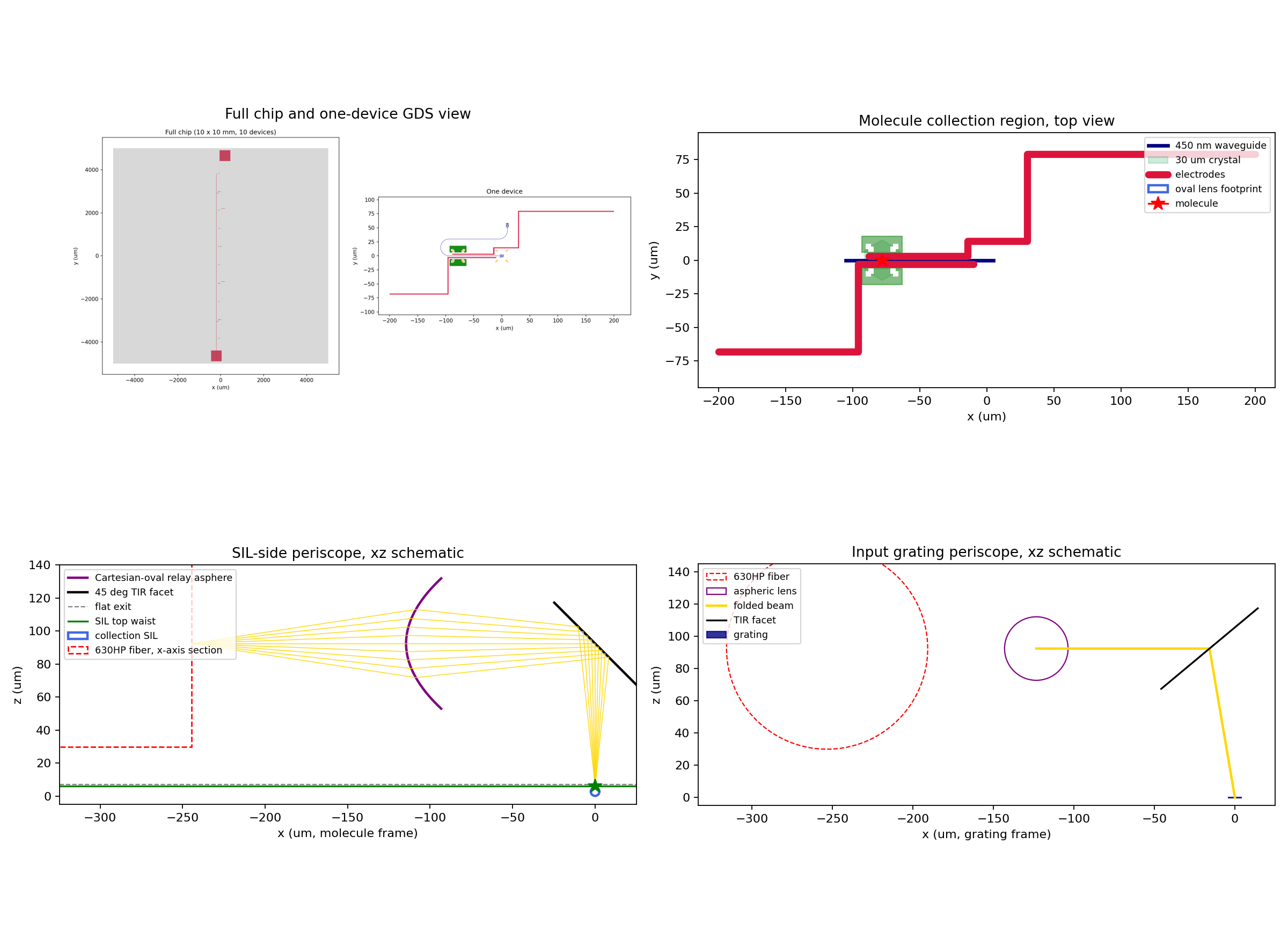
The assembled v1 device: input grating+periscope, chip GDS, collection lens+SIL periscope, and the pre-fabrication master report.
Generated from the consolidated tree single_molecule_device_v1.
Executive Summary
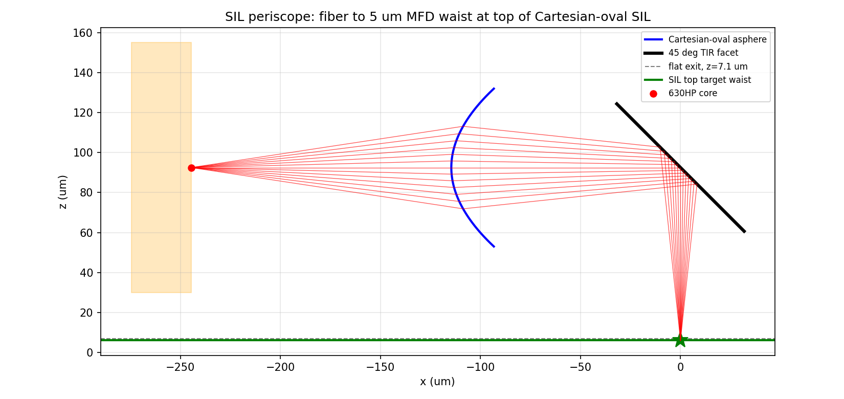
This package consolidates the input grating/periscope, chip GDS, molecule collection lens, and SIL-side collection periscope into one pre-fabrication review tree. Current single wavelength results are:
| Metric | Value |
|---|---|
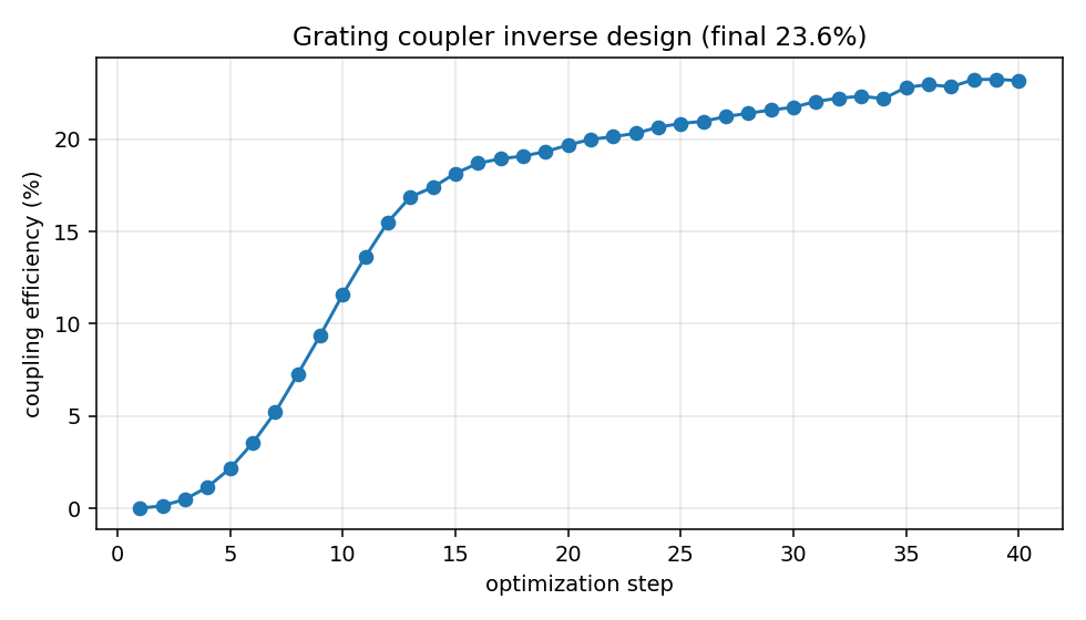
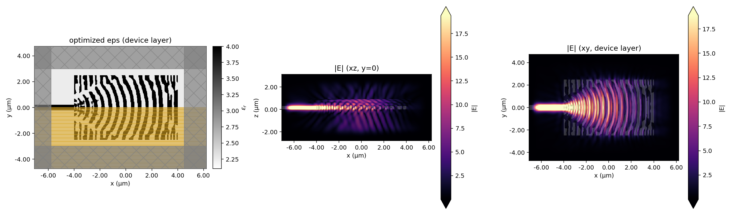
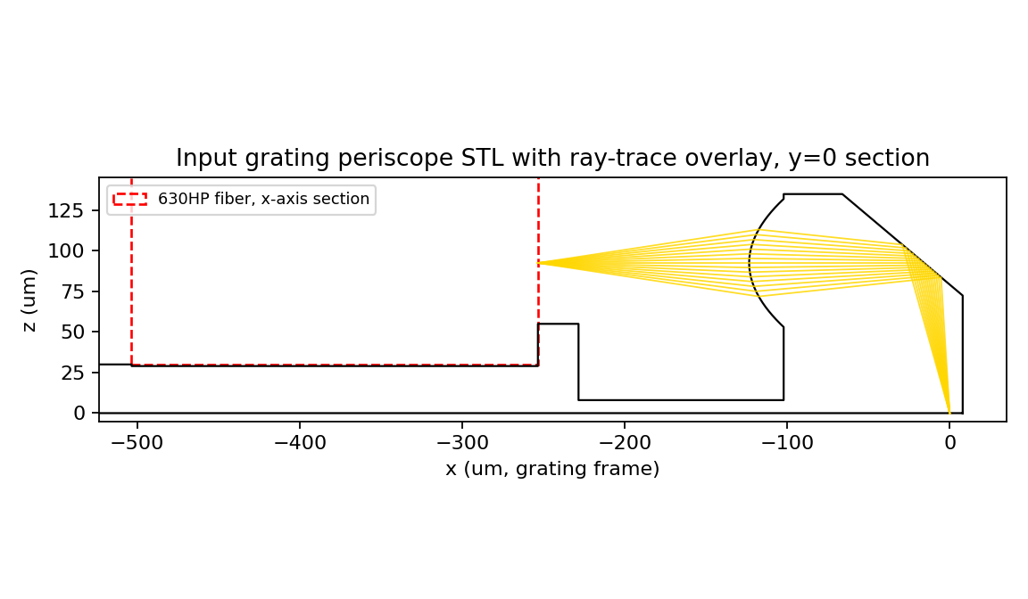
| Input grating coupling at 780 nm | 23.58% |
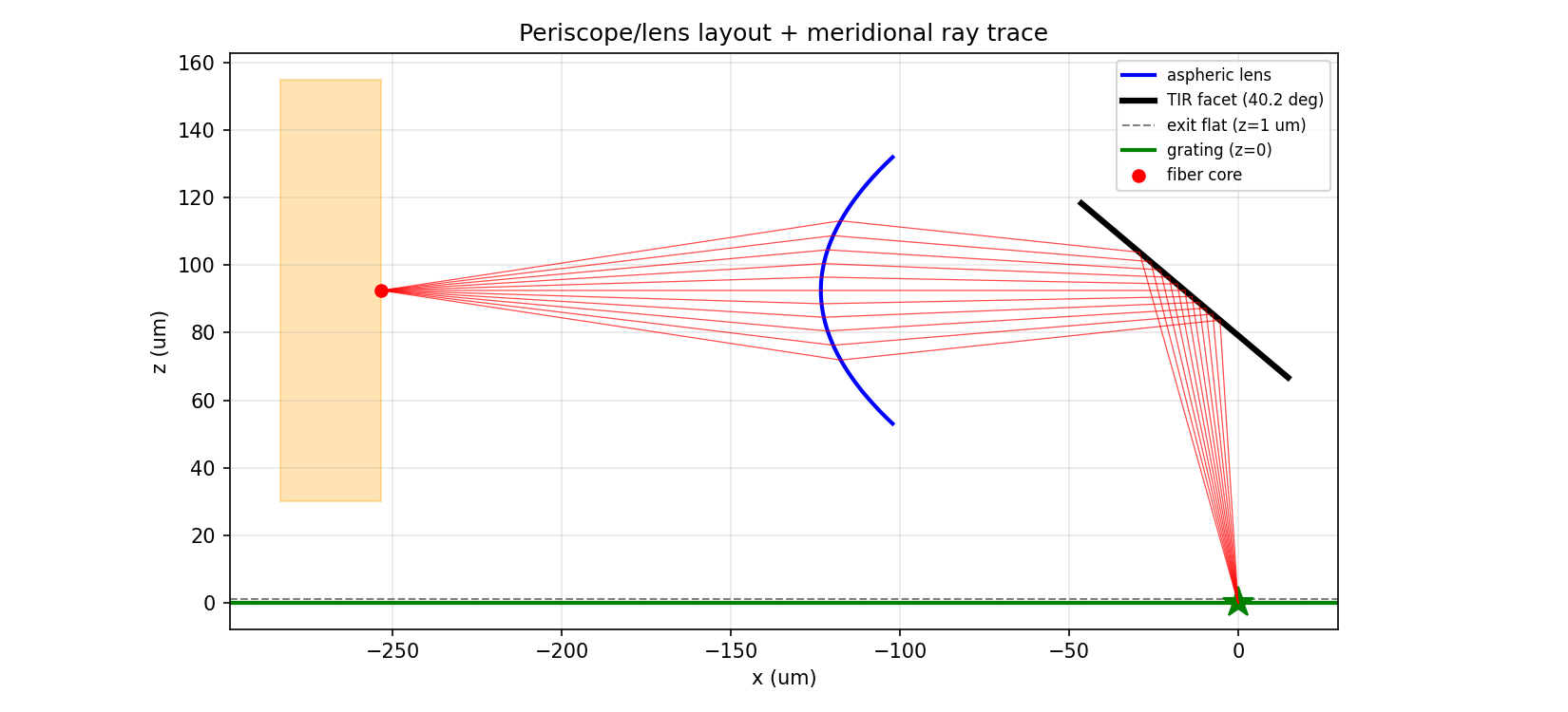
| Input periscope geometric RMS spot | 1.24 nm |
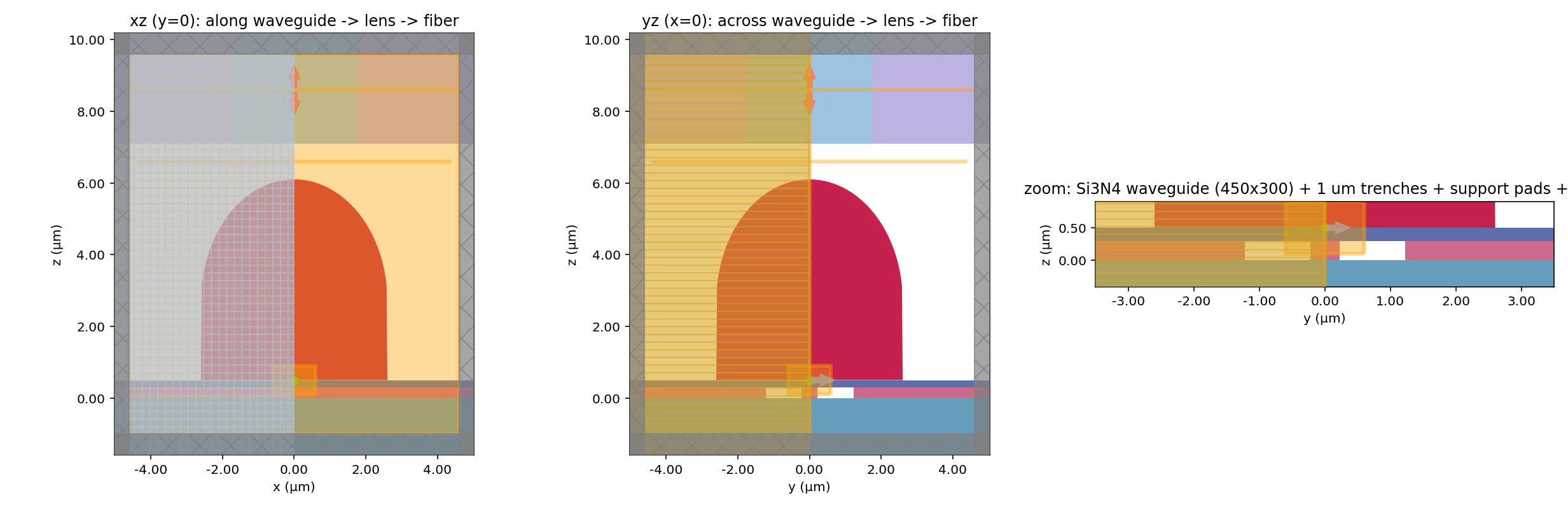
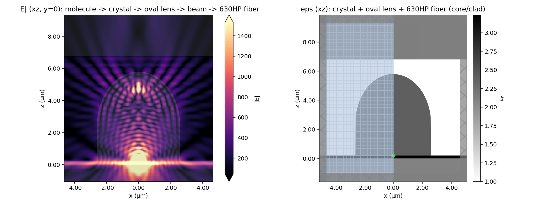
| Collection lens coupling to 630HP at 780 nm | 10.10% |
| Collection upward power fraction | 17.86% |
| Collection periscope target MFD | 5.00 um |
| Collection periscope geometric RMS spot | 18.31 nm |
Master Parameters
{
  "lambda_nm": 780,
  "indices": {
    "SiN": 2.0,
    "SiO2": 1.45,
    "PVA": 1.5,
    "resist": 1.55,
    "crystal": 1.8
  },
  "stack_um": {
    "waveguide": 0.3,
    "crystal": 0.2,
    "PVA cap": 1.0
  },
  "grating": {
    "MFD_um": 5.0,
    "angle_deg": 10.0,
    "design_region_um": [
      8.0,
      5.0
    ],
    "pixel_nm": 30,
    "min_feature_nm": 120
  },
  "fiber_630HP": {
    "r_core_um": 1.75,
    "NA": 0.12,
    "n_core": 1.461933309012419,
    "n_clad": 1.457,
    "MFD_um": 5.0
  },
  "chip": {
    "size_mm": 10.0,
    "n_devices": 10,
    "pitch_um": 500.0,
    "device_span_um": 4500.0,
    "electrode_highway_x_um": {
      "positive": 200.0,
      "negative": -240.0
    },
    "bond_pad_um": [
      5000.0,
      2000.0
    ],
    "bond_pad_edge_clearance_um": 100.0,
    "electrode_highway_width_um": 50.0,
    "electrode_active_width_um": 1.5,
    "support_stack_um": {
      "waveguide_to_inner_strip_gap": 1.5,
      "inner_strip": 2.0,
      "strip_to_electrode_gap": 1.5,
      "electrode_to_outer_support_gap": 1.5
    },
    "bend_radius_um": 15.0,
    "wg_width_nm": 450
  },
  "alignment_marks": {
    "layer": 10,
    "grating_l_outer_corner_bbox_um": [
      30.0,
      40.45
    ],
    "grating_l_arm_width_um": [
      10.0,
      2.0
    ],
    "molecule_alignment": "support_pad_edges"
  },
  "chip_lithography_crosses": {
    "main_size_um": 200.0,
    "main_stroke_um": 5.0,
    "main_positions_um": [
      [
        -3900.0,
        -3700.0
      ],
      [
        3900.0,
        -3700.0
      ],
      [
        -3900.0,
        3700.0
      ],
      [
        3900.0,
        3700.0
      ]
    ],
    "backup_size_um": 80.0,
    "backup_stroke_um": 3.0,
    "backup_positions_um": [
      [
        -3900.0,
        -2700.0
      ],
      [
        3900.0,
        -2700.0
      ],
      [
        -3900.0,
        2700.0
      ],
      [
        3900.0,
        2700.0
      ]
    ],
    "layer": 10
  },
  "print_overlay_layers": {
    "sil_lens": 20,
    "input_periscope": 21,
    "input_u_groove": 22,
    "collection_periscope": 23,
    "collection_u_groove": 24,
    "u_groove_alignment_marks": 10
  },
  "lens": {
    "h_apex_um": 5.6,
    "rho_max_um": 2.6007540384718144,
    "kappa": 4.636363636363636
  },
  "nanoscribe_25x_IPDip": {
    "print_field_um": 270.0,
    "min_feature_um": 0.2,
    "min_wall_um": 1.0
  }
}
Architecture
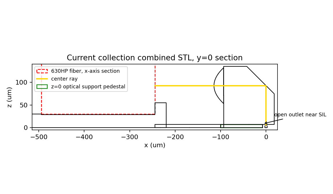
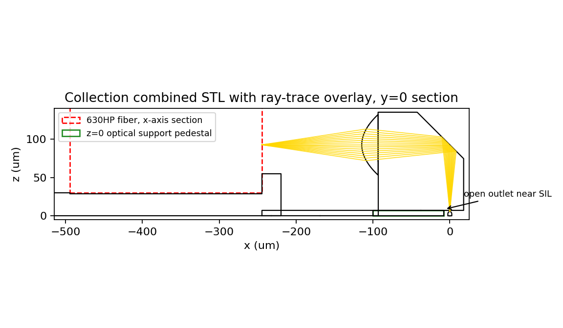
input/: inverse-designed grating coupler and grating-side fiber periscope.chip/: 10-device nanophotonic GDS array with waveguides, support pads, electrodes, alignment marks, and grating instances.collection/: Cartesian-oval collection lens FDTD files and SIL-side periscope.deliverables/: current ship-to-fab files gathered in one place.verification/: local no-cost pre-fab checks.
Input Grating and Periscope
Chip and Nanophotonics
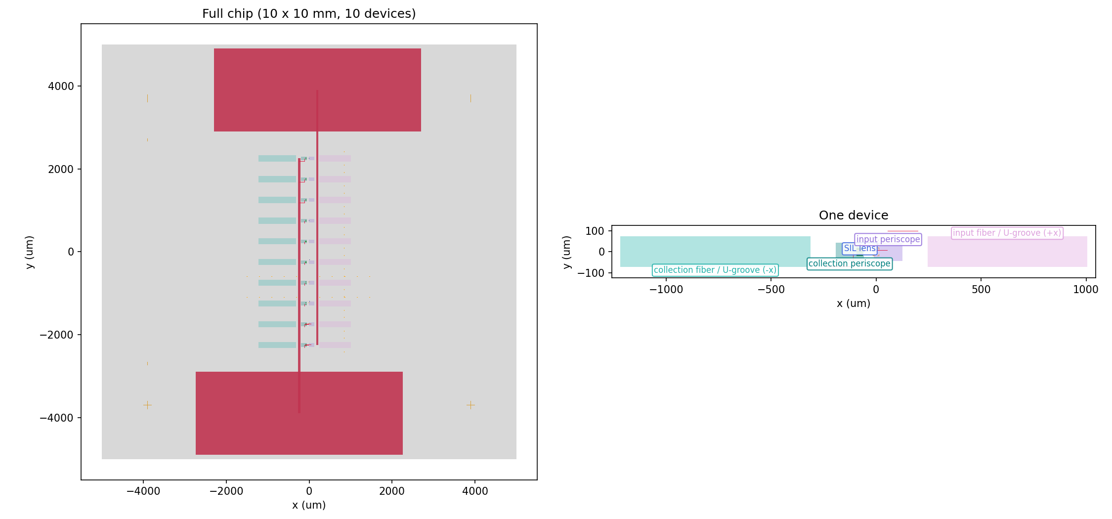
GDS overlap check:
{
  "available": true,
  "electrode_sin_intersection_um2": 0.0,
  "pad_sin_intersection_um2": 0.0,
  "mark_sin_intersection_um2": 0.0,
  "mark_pad_intersection_um2": 0.0,
  "mark_electrode_intersection_um2": 0.0,
  "status": "PASS",
  "failures": {}
}
Collection Lens and SIL-Side Periscope
Verification
Ray/STL Checks
{
  "input_periscope": {
    "mesh": "input\\stl\\periscope_mount.stl",
    "all_points_inside_bbox": true,
    "min_margin_to_bbox_low_um": [
      750.0,
      72.5,
      0.0
    ],
    "min_margin_to_bbox_high_um": [
      7.99,
      72.5,
      21.833
    ],
    "status": "PASS",
    "rays_traced": 15
  },
  "collection_periscope": {
    "mesh": "collection\\stl\\collection_combined.stl",
    "all_points_inside_bbox": true,
    "min_margin_to_bbox_low_um": [
      750.0,
      72.5,
      6.1
    ],
    "min_margin_to_bbox_high_um": [
      9.74,
      72.5,
      21.832
    ],
    "status": "PASS",
    "rays_traced": 15
  }
}
Fabrication Heuristic
| Part | Rating | Extents (um) | 25x fields xyz | Notes |
|---|---|---|---|---|
| input_periscope | yellow | [1011.4, 145.0, 134.951] |
[4, 1, 1] |
larger than one 25x IP-Dip field; estimated stitch fields [4, 1, 1]; contains mesh edges below 0.2 um; this may be tessellation, not a fabricated feature |
| collection_lens | green | [5.202, 5.202, 5.6] |
[1, 1, 1] |
contains mesh edges below 0.2 um; this may be tessellation, not a fabricated feature |
| collection_optical | green | [132.55, 86.903, 134.951] |
[1, 1, 1] |
contains mesh edges below 0.2 um; this may be tessellation, not a fabricated feature |
| collection_support | yellow | [901.262, 145.0, 134.382] |
[4, 1, 1] |
larger than one 25x IP-Dip field; estimated stitch fields [4, 1, 1] |
Interpretation:
green: fits one 25x IP-Dip field and is watertight.yellow: watertight but needs stitch/split/process review.red: missing, non-watertight, or below feature heuristic.
Deliverables
| File | Bytes | SHA256 prefix |
|---|---|---|
deliverables/chip.gds |
53,274 | 576d75f2af94fbbb |
deliverables/input_periscope.stl |
611,084 | 43e8f6d566dab2d0 |
deliverables/collection_lens.stl |
1,666,084 | 5fc0175e77d7a31e |
deliverables/collection_optical.stl |
2,244,984 | 482d69d64d3c6f36 |
deliverables/collection_support.stl |
30,884 | ae9596ea6364c033 |
deliverables/fabrication_notes.md |
1,105 | ce356f5ca402fa07 |
Current Gaps Before Final Fabrication
- Wavelength sweeps for grating and collection lens are not yet run in this consolidated tree. They require explicit FlexCredit approval.
- The collection split STLs are a practical optical/support split, but the mating interface is not yet a fully engineered kinematic pin/slot system.
- The full periscope assemblies are ray-optics validated, not full-FDTD validated.
- Existing collection FDTD uses an
Eydipole; no polarization sweep has been run. - Some older component reports remain in
input/andcollection/; this top-level report plusshared/design_params.pyare authoritative for pre-fab review.
Reproduction
python make_master_report.py
python verification\intersection_check.py
python verification\stl_clip_check.py
python verification\stl_fabrication_check.py
Appendix source reports:
input/grating_report.mdinput/periscope_report.mdcollection/lens_report.mdverification/consistency_audit.mdverification/alignment_tolerance.md
Downloads
These are the ship-to-fab files gathered in deliverables/ per the master report's manifest table.
Source: device_architectures/v1/single_molecule_device_v1/