DBT TIR-SIL fiber coupler v1
Waveguide -> printed IP-S TIR-SIL -> 630HP fiber mode coupling workflow.
Tidy3D workflow for coupling an x-oriented DBT dipole through a waveguide stack, a printed IP-S TIR-SIL, and into a 630HP-like fiber mode.
This version is rebuilt around the workflow in:
G:\Shared drives\QLuster\product\v1\tidy3d-out-of-plane\solid_immersion_lens_v6\v6.ipynb
The script follows the same structure as that notebook: build the lens mesh,
build the Tidy3D simulation, solve/check the fiber mode, run the forward FDTD
job, compute coupling as |a_fiber,+|^2 / flux_dip, export STL, and write a
Markdown report with geometry, field, mode, and coupling plots.
Files
tir_sil_simulation.pycontains the full simulation/report workflow.stl/receives generated IP-S TIR-SIL STL files.reports/receives timestamped reports, figures, simulation files, and result JSON.
Geometry
- SiO2 substrate,
n = 1.44 - 450 nm x 300 nm Si3N4 waveguide,
n = 2.0 - Air beside the waveguide in the waveguide layer
- 200 nm DBT-host crystal film,
n = 1.8 - x-oriented point dipole on the crystal top surface
- IP-S TIR-SIL with a central direct lens plus annular TIR reflector
- The direct lens branch is explicitly limited to rays whose lens-air incidence is below the IP-S/air critical angle with a configurable margin.
- The report includes angular coverage accounting so unassigned source-ray angles are visible instead of silently ignored.
- 630HP-like fiber modeled as a step-index core/cladding above the optic
Usage
Dry-run the geometry, STL, simulation object, and report without spending Tidy3D credits:
Run the full fiber-coupling simulation:
Sweep the lower TIR source-ray cutoff angle:
Useful geometry knobs:
--direct-lens-apex-height-um--direct-lens-theta-max-deg--direct-lens-tir-margin-deg--tir-theta-min-deg--tir-theta-max-deg--tir-parabola-constant-um--fiber-gap-um
Results
First sweep point (32.0deg wall, baseline)
DBT TIR-SIL Fiber Coupler v1 Report
- Generated:
2026-05-28T15:40:08 - Status: dry run only
- STL:
stl/tir_sil_wall_32.0deg.stl - Simulation file:
reports/data/simulation_20260528_153959_wall_32p0deg.hdf5
Geometry
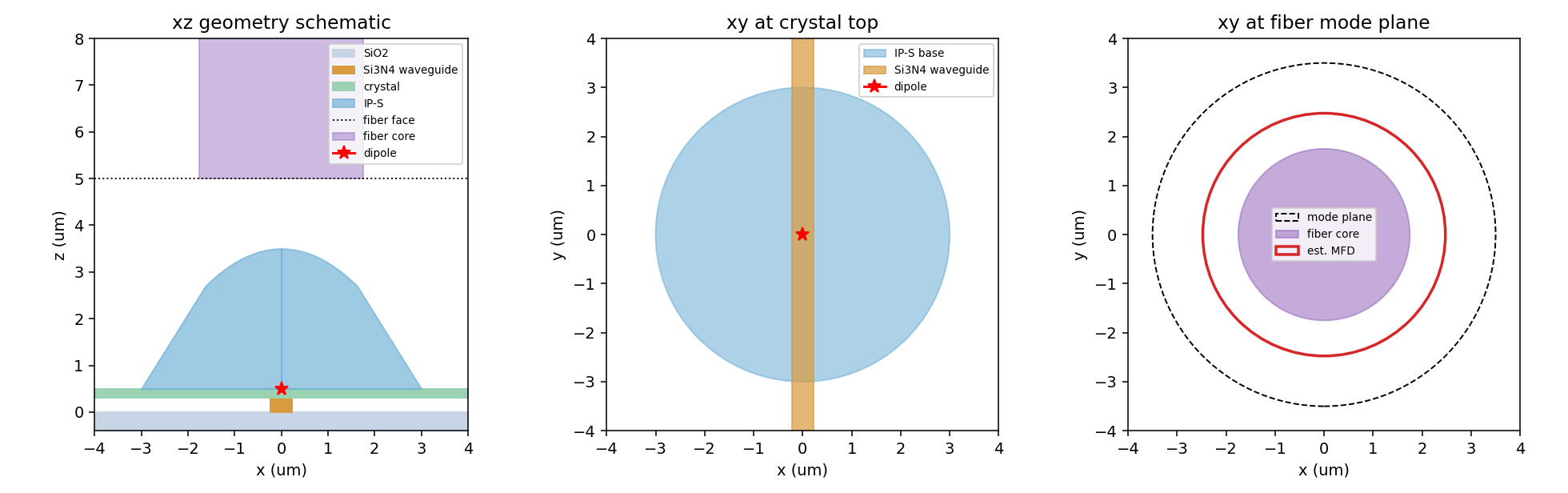
Coordinate convention: z = 0 is the SiO2 top surface and the Si3N4 waveguide bottom.
The DBT molecule is modeled as a point dipole at the crystal top surface:
z = 0.500 um.
- SiO2 substrate:
n = 1.440 - Si3N4 waveguide: width
0.450 um, thickness0.300 um,n = 2.000 - Lateral material beside waveguide: air,
n = 1.000 - DBT host crystal film: thickness
0.200 um,n = 1.800, infinite x/y extent in the simulation - IP-S TIR-SIL:
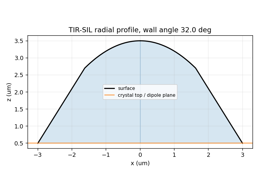
n = 1.515, base radius3.000 um, height3.000 um, wall angle32.00 deg - IP-S/air critical angle:
41.30 degmeasured from the surface normal
Fiber Target
The fiber target is Thorlabs 630HP. Thorlabs specifies 630HP as a 600-770 nm
single-mode fiber with mode-field diameter 4.0 +/- 0.5 um @ 630 nm.
The simulation wavelength is 780 nm, which is slightly outside that listed
630HP operating band, so the 780 nm MFD is treated as an estimate here.
This first-pass model uses a 630HP-like step-index fiber stub:
- Cladding radius:
62.5 um - Core radius:
1.750 um - NA:
0.120 - Cladding index:
1.4533 - Derived core index:
1.4582 - Estimated 780 nm MFD used for monitor sizing:
4.95 um - Mode monitor plane:
z = 6.650 um, width6.400 um
Simulation
- Center wavelength:
0.7800 um - Wavelength samples:
3 - Simulation window:
8.00 x 8.00 x 10.60 um - Grid: Tidy3D auto grid, min
16steps per wavelength - Dipole polarization:
Ex - Run time:
7.500e-13 s - Estimated cost:
nanFlexCredits - Real cost:
nanFlexCredits
Field Plots
Field plots are generated after a full Tidy3D run.
Fiber-Mode Signal
Simulation was not run because --dry-run was used.
Parameters
{
  "wavelength_um": 0.78,
  "bandwidth_um": 0.02,
  "n_wavelengths": 3,
  "n_air": 1.0,
  "n_sio2": 1.44,
  "n_sin": 2.0,
  "n_crystal": 1.8,
  "n_ips": 1.515,
  "fiber_mfd_spec_um_at_630": 4.0,
  "fiber_mfd_est_um_at_780": 4.95,
  "fiber_clad_radius_um": 62.5,
  "fiber_core_radius_um": 1.75,
  "fiber_na": 0.12,
  "fiber_clad_index": 1.4533,
  "fiber_gap_um": 1.5,
  "fiber_stub_um": 3.0,
  "substrate_thickness_um": 1.0,
  "waveguide_width_um": 0.45,
  "waveguide_thickness_um": 0.3,
  "crystal_thickness_um": 0.2,
  "tir_wall_angle_deg": 32.0,
  "tir_base_radius_um": 3.0,
  "tir_cone_height_um": 2.2,
  "tir_cap_sag_um": 0.8,
  "tir_profile_points": 180,
  "tir_angular_points": 160,
  "sim_xy_um": 8.0,
  "pml_pad_um": 0.8,
  "min_steps_per_wvl": 16,
  "run_time_s": 7.5e-13,
  "monitor_plane_xy_um": 7.0,
  "source_polarization": "Ex",
  "tir_height_um": 3.0,
  "tir_apex_z_um": 3.5,
  "fiber_face_z_um": 5.0,
  "fiber_core_index": 1.4582458263269606,
  "ips_air_critical_angle_deg": 41.30490702409531
}
Source Notes
- Nanoscribe IP-S refractive index was taken from Nanoscribe's printing-materials product folder:
n = 1.515at 589 nm and 20 C: https://www.nanoscribe.com/fileadmin/Nanoscribe/PDF/Product-folder/Folder-Printing-Materials.pdf Dispersion at 780 nm should be replaced by measured data if available. - 630HP MFD was taken from Thorlabs' 630HP table:
4.0 +/- 0.5 um @ 630 nm. https://www.thorlabs.com/newgrouppage9.cfm?objectgroup_id=949&pn=630HP The 780 nm value here is a simple wavelength-scaled estimate for monitor sizing, not a vendor specification. - TIR-SIL starting point: https://arxiv.org/abs/2007.06369
Latest sweep point (final)
DBT Waveguide TIR-SIL Fiber Coupling Report
- Generated:
2026-05-29T08:26:20 - Status: dry run only
- Reference implementation style:
tidy3d-out-of-plane/solid_immersion_lens_v6/v6.ipynb - Cost-estimate task:
fdve-2ad3547f-fd3e-47b9-9a77-9d9fd040fe59 - STL:
stl/tir_sil_waveguide_tir40p5_C2p00_m7_Ex.stl - Simulation file:
reports/data/simulation_20260529_082608_tir40p5_C2p00_m7_Ex.hdf5
Geometry
- SiO2 substrate:
n = 1.440, simulated thickness1.000 um - Si3N4 waveguide:
n = 2.000, width0.450 um, thickness0.300 um - Air beside the waveguide in the waveguide layer
- DBT host crystal:
n = 1.800, thickness0.200 um - Dipole position:
(0, 0, 1.500000) um, exactly on the crystal top surface - Dipole orientation: x direction (
Ex) - IP-S TIR-SIL index:
n = 1.515 - Fiber: core radius
1.750 um, cladding index1.4533, derived core index1.4582, NA0.120
TIR-SIL Ray Design
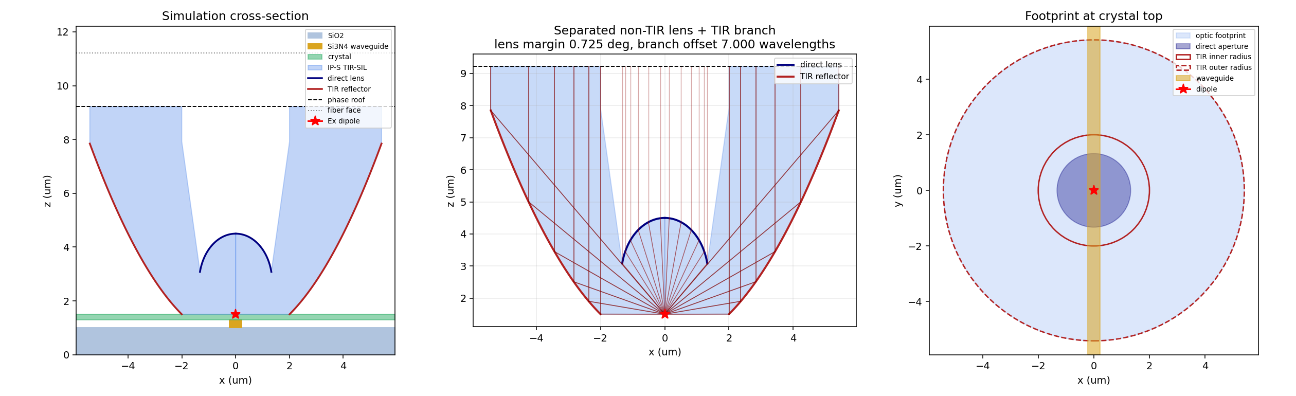
The central branch is a Cartesian-oval direct lens for low-angle rays
whose incidence at the IP-S/air lens surface is safely below the
critical angle. Rays that would TIR at that refractive surface are not
assigned to the central branch. The raised annular branch is the
reflection-law surface with local normal parallel to k_in - zhat.
For the implemented vertical output beam this integrates to the
paraboloid condition s - z = C, with the emitter at the focus. The
annular roof height is then chosen so the direct and TIR branches differ
by an integer number of wavelengths at 780 nm.
- Direct-lens source angles:
0to40.00 deg - Direct-lens radius:
1.326 um - Max direct-lens internal incidence:
40.5800 deg - Direct-lens margin to critical angle:
0.7249 deg(required margin0.0010 deg) - TIR source angles:
40.50to89.90 deg - TIR radii:
2.003to5.421 um - TIR incidence range:
45.0500to69.7500 deg - IP-S/air critical angle:
41.3049 deg - Single-bounce vertical TIR source-angle upper limit:
97.39 deg - Minimum TIR-surface margin above critical:
3.7451 deg - TIR reflection-law error: max
4.965e-16, rms1.923e-16against+z - Unassigned source-angle gap:
0.500 deg - Accounted solid-angle fraction of upper hemisphere:
99.26%(direct23.40%, TIR75.87%, gap0.5638%) - Direct-branch OPL variation:
1.776e-15 um - TIR-branch OPL variation:
7.994e-14 um - Branch phase offset:
7.000000wavelengths (m = 7)
Simulation
- Wavelength range:
0.750to0.810 umwith31samples - Simulation size:
11.842 x 11.842 x 12.218 um - Transverse domain rule: optic diameter
10.842 umplus1.000 um - Simulated substrate thickness:
1.000 um - Simulated fiber length above fiber face:
1.000 um - Symmetry:
(-1, 1, 0)(Exdipole: odd in x, even in y) - Grid: auto, min
15steps per wavelength - Mode monitor z:
11.718 um - Mode monitor plane:
8.500 x 8.500 um - Flux monitor:
flux_dip, same normalization pattern as v6 - Field plot: Tidy3D
sim_data.plot_field('field_xz', 'E', 'abs^2')at the center-frequency field monitor; no time-step selection is involved - Estimated cost:
0.6962411590749145FlexCredits - Real cost:
nanFlexCredits
Results
Simulation was not run because --dry-run was used.
Field plots are generated after a full Tidy3D run.
Parameters
{
  "wl_um": 0.78,
  "bw_um": 0.06,
  "n_wl": 31,
  "n_air": 1.0,
  "n_sio2": 1.44,
  "n_sin": 2.0,
  "n_crystal": 1.8,
  "n_sil": 1.515,
  "n_fiber_clad": 1.4533,
  "fiber_na": 0.12,
  "t_sio2_um": 1.0,
  "waveguide_width_um": 0.45,
  "waveguide_thickness_um": 0.3,
  "crystal_thickness_um": 0.2,
  "fiber_core_radius_um": 1.75,
  "fiber_clad_diameter_um": 125.0,
  "fiber_gap_um": 2.0,
  "fiber_stub_um": 1.0,
  "direct_lens_apex_height_um": 3.0,
  "direct_lens_theta_max_deg": 40.0,
  "direct_lens_tir_margin_deg": 0.001,
  "tir_theta_min_deg": 40.5,
  "tir_theta_max_deg": 89.9,
  "tir_parabola_constant_um": 2.0,
  "tir_roof_clearance_um": 0.8,
  "transition_clearance_um": 0.08,
  "direct_profile_points": 120,
  "tir_profile_points": 120,
  "angular_segments": 144,
  "min_steps_per_wvl": 15,
  "run_time_s": 5e-12,
  "pml_spacing_um": 0.46799999999999997,
  "sim_xy_um": 0.0,
  "domain_margin_um": 1.0,
  "mode_plane_um": 8.5,
  "eff_inf_um": 10.0,
  "source_polarization": "Ex",
  "n_fiber_core": 1.4582458263269606,
  "z_substrate_top_um": 1.0,
  "z_waveguide_top_um": 1.3,
  "z_crystal_top_um": 1.5,
  "z_emitter_um": 1.5,
  "z_roof_um": 9.21844660194175,
  "z_fiber_face_um": 11.21844660194175,
  "z_mode_monitor_um": 11.71844660194175,
  "domain_xy_um": 11.842474437339622,
  "optic_outer_radius_um": 5.421237218669811,
  "direct_lens_radius_um": 1.3259890361204258,
  "direct_lens_edge_z_um": 3.0802521975370514,
  "tir_inner_radius_um": 2.0034937082264417,
  "tir_outer_radius_um": 5.421237218669811,
  "tir_z_max_um": 7.847453245272696,
  "phase_report": {
    "direct_opl_mean_um": 9.26344660194175,
    "direct_opl_ptp_um": 1.7763568394002505e-15,
    "tir_opl_mean_um": 14.723446601941752,
    "tir_opl_ptp_um": 7.993605777301127e-14,
    "branch_opl_delta_um": 5.460000000000003,
    "branch_phase_offset_wavelengths": 7.0000000000000036,
    "phase_order": 7,
    "direct_lens_incidence_max_deg": 40.579977333803406,
    "direct_lens_incidence_margin_to_critical_deg": 0.7249296902919014,
    "direct_lens_tir_margin_required_deg": 0.001,
    "tir_incidence_min_deg": 45.05000000000002,
    "tir_incidence_max_deg": 69.75,
    "tir_incidence_min_margin_above_critical_deg": 3.7450929759047114,
    "critical_angle_deg": 41.30490702409531,
    "single_bounce_vertical_tir_source_angle_max_deg": 97.39018595180939,
    "tir_reflection_direction_error_max": 4.965068306494546e-16,
    "tir_reflection_direction_error_rms": 1.9229626863835638e-16,
    "unassigned_source_angle_gap_deg": 0.5,
    "direct_solid_angle_fraction_upper_hemisphere": 0.233955556881022,
    "gap_solid_angle_fraction_upper_hemisphere": 0.005638477518947083,
    "tir_solid_angle_fraction_upper_hemisphere": 0.7586606372341327,
    "total_accounted_solid_angle_fraction_upper_hemisphere": 0.9926161941151547
  }
}
20 additional parametrized sweep reports exist under reports/.
Downloads
tir_sil_wall_32.0deg.stltir_sil_phase_matched_theta84p5_C2p20_m5.stltir_sil_phase_matched_theta85p0_C2p20_m5.stltir_sil_waveguide_tir40p5_C2p00_m7_Ex.stltir_sil_waveguide_tir55p5_C4p00_m10_Ex.stltir_sil_waveguide_tir60p0_C4p00_m9_Ex.stltir_sil_waveguide_tir82p7_C2p00_m5_Ex.stltir_sil_waveguide_tir84p0_C2p00_m5_Ex.stltir_sil_waveguide_tir87p0_C2p00_m5_Ex.stl
Source: nanophotonic_devices/fiber_collection_optics/dbt_tir_sil_fiber_coupler_v1/