Gen-2 lens codesign (collect/dual/lens)¶
Active gen-2 R&D: emitter-lens codesign, TiO2/asphere inverse design, dual-decoupled lens variant. Not yet assembled into a device_architectures/v2 chip.
No top-level README -- this is stage 1 (escape cone + IP-S lens exploration) of the v2 codesign; stage 2 and stage 3 results are appended below.
Single-molecule upward-collection device, v2 Date: 2026-06-04 · Status: lens + cavity sweeps RAN (~3 FC) — η_fiber 8.1% → 25.5% with the PEC mirror
0. Executive summary¶
This is the first exploratory stage of the v2 device. The full stack is
Gold mirror → SiO2 spacer → TiO2 inverse-design structure
   → n=1.8 crystal (200 nm, dipole in the middle)
   → IP-S solid-immersion / collection lens → 1 µm air → 630HP fiber
The end goal is to maximise α(F_P)·η, where α is the (Purcell-enhanced) zero-phonon-line branching ratio and η is the collection efficiency into the 630HP fiber mode.
Per the agreed staging, this stage does only the parts that can be settled before the TiO2 inverse design:
- Escape cone anthracene (n=1.8) → IP-S (n=1.51).
- Analytic lens that converts that escape cone into the 630HP fiber mode, parametrised
by a single sweep knob (apex height
H_APEX). - A dry-run FDTD
dipole → crystal → lens(H_APEX) → 1 µm air → 630HP fiberready to sweepH_APEXfor maximum coupling — geometry built, cost estimated, not run. - The objective function and the Purcell→α framework that the later TiO2 inverse design will optimise.
Key numbers
| Quantity | Value |
|---|---|
| Design wavelength | 780 nm (anthracene/DBT ZPL) |
| Escape-cone half-angle θ_c (crystal→IP-S) | 57.0° |
| Conserved NA of escaping light (= n·sinθ_c = n_IP-S) | 1.51 |
| Emission crossing into IP-S within the cone (Ey dipole, Fresnel-weighted) | ≈ 26 % (no mirror yet) |
| Intrinsic ZPL branching α₀ | ⅓ |
| Lens: Cartesian-oval conic κ | 4.922 |
| Lens aperture radius ρ_max (H_APEX = 6 µm) | 2.70 µm |
| FDTD cost / point (lens sweep) | 0.111 FC (18.0 M cells) |
| 7-point H_APEX sweep total | ≈ 0.78 FC (spent) |
| Lens H_APEX (no-mirror sweep optimum) | 4.5 µm |
| η into 630HP mode, no mirror | 8.1 % |
| + PEC mirror cavity, no TiO₂ (spacer 0.04 / H_APEX 3.5 / gap 1.5) | η_fiber = 25.5 %, η_up = 41 % |
| + PEC mirror cavity WITH 150 nm TiO₂ film (spacer 0.04) | η_fiber = 29.3 %, η_up = 45.8 % |
1. Escape cone: anthracene crystal → IP-S¶
Light leaves the crystal into the IP-S lens through a planar high-index interface. Total internal reflection sets the escape-cone half-angle
θ_c = arcsin(n_IP-S / n_crystal) = arcsin(1.51 / 1.80) = 57.02°
Because n·sinθ is conserved across the interface, the marginal escaping ray has
NA = n_crystal·sin θ_c = n_IP-S = 1.51
i.e. the escaping light fills the full IP-S hemisphere up to grazing. This is exactly the solid-immersion advantage: putting IP-S (rather than air) directly on the crystal lets us collect rays out to a crystal-side angle of 57° instead of the 33.7° we would get for a crystal/air interface.
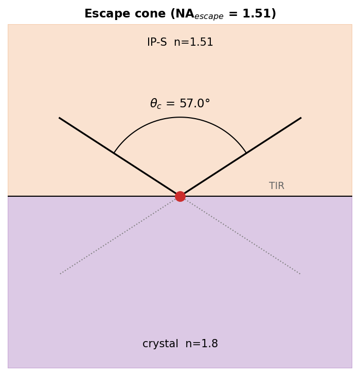 Escape cone at the crystal/IP-S interface. Rays inside 57° transmit; steeper rays are
totally internally reflected.
Escape cone at the crystal/IP-S interface. Rays inside 57° transmit; steeper rays are
totally internally reflected.
How much light is actually in the cone? Using the full classical radiation pattern of an in-plane (Ey) dipole, weighted by the Fresnel power transmission (s and p) across the crystal/IP-S interface:
| Emitter | Geometric cone fraction | Fresnel-weighted into IP-S |
|---|---|---|
| In-plane (Ey) dipole | 27.6 % | 26.1 % |
| Isotropic (reference) | 22.8 % | 21.6 % |
This is the fraction of total emission that reaches the IP-S within the escape cone, for a bare crystal on SiO2. It is the analytic ceiling that the lens can collect at this stage. It excludes three things the FDTD will add later: the gold mirror (reflects the downward half back up — can roughly double the upward fraction), the modified LDOS / Purcell factor from the TiO2 cavity, and the finite lens aperture.
2. The IP-S collection lens (analytic)¶
2.1 Why a single Cartesian-oval surface¶
The lens has one optical job: take the diverging emission inside the IP-S and deliver it to the 630HP fiber 1 µm away, whose mode is a Gaussian of MFD ≈ 5 µm (waist radius ≈ 2.5 µm), divergence NA ≈ 0.12. A single refracting IP-S/air surface shaped as a Cartesian oval images a point source stigmatically (zero spherical aberration) — no multi-element optics needed, and it prints in one shot on the Nanoscribe.
In the collimating limit the surface height is
h(ρ) = [ n_air·H_APEX + n_IP-S·√(H_APEX² − κρ²) ] / (n_IP-S + n_air), κ = (n_IP-S + n_air)/(n_IP-S − n_air) = 4.922, valid for ρ ≤ ρ_max = H_APEX/√κ.
The lens is flat-bottomed: it sits directly on the crystal across its full aperture (radius ρ_max), so the entire footprint is a crystal/IP-S interface (the 57° escape cone), not crystal/air. The oval cap forms the top; a short vertical wall closes the side.
⚠ Design fix vs v1. The v1 lens mesh tapered to a cone point at its base, so IP-S touched the crystal only on-axis and most rays would have hit a crystal/air interface (33.7° cone). The v2 mesh is flat-bottomed so the escape-cone physics is the real one.
2.2 The single sweep parameter¶
H_APEX (apex height above the lens base) sets both the aperture ρ_max = H_APEX/√κ and the
output beam. For H_APEX ≈ 6 µm:
- aperture radius ρ_max = 2.70 µm,
- the quasi-collimated output beam has waist ≈ ρ_max and divergence ≈ λ/(π·ρ_max) ≈ 0.09 rad,
which matches the 630HP mode (waist 2.5 µm, NA 0.12) across the 1 µm gap. Larger H_APEX collects a wider angular range but over-fills the fiber; smaller under-fills. The geometric optimum is therefore near H_APEX ≈ 6 µm, and the FDTD sweep finds the true mode-overlap optimum (which differs from the geometric one because the fiber is mode-matched, not just spot-matched).
3. Lens-coupling FDTD (dry run)¶
3.1 Geometry¶
SiO2 (semi-infinite, z<0)          [spacer/substrate; gold mirror + TiO2 deliberately
                                    omitted at this stage to isolate the lens shape]
crystal  n=1.8   z ∈ [0, 0.20]     Ey point dipole at z = 0.10 (mid-plane)
IP-S lens n=1.51  flat base on crystal, apex at z = 0.20 + H_APEX
1 µm air gap
630HP fiber  (core R=1.75 µm, n_core=1.462; cladding n=1.457), facet 1 µm above apex
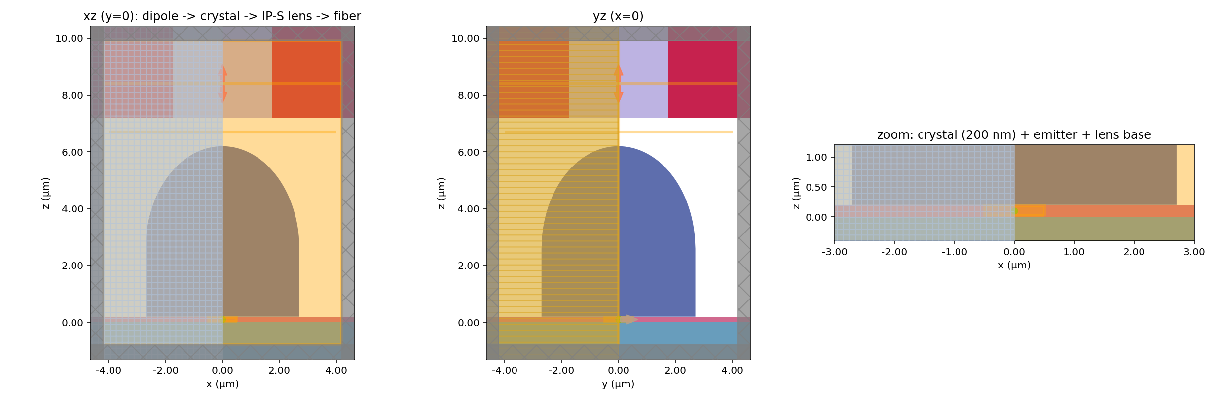 Left: xz along the optical axis (dipole → crystal → flat-bottomed IP-S oval → air gap →
fiber). Middle: yz. Right: zoom on the 200 nm crystal, the mid-plane emitter, and the lens
base sitting flush on the crystal. The fiber core/cladding run continuously through the top
PML.
Left: xz along the optical axis (dipole → crystal → flat-bottomed IP-S oval → air gap →
fiber). Middle: yz. Right: zoom on the 200 nm crystal, the mid-plane emitter, and the lens
base sitting flush on the crystal. The fiber core/cladding run continuously through the top
PML.
3.2 Objective function (this stage)¶
For the lens-shape sweep there is no engineered Purcell yet, so we simply maximise the collection efficiency into the real fiber mode:
η_collect = P(630HP LP01 mode) / P(total emitted)
computed by real mode matching — a ModeMonitor solves the actual 630HP LP01 mode inside
the fiber and we take |mode amplitude|². The denominator is the dipole's total emitted power
from a closed flux box around the emitter. We also report η_up (upward power / total) for
diagnostics.
3.3 Cost¶
| Item | Value |
|---|---|
| Domain | 8.41 × 8.41 × 10.70 µm |
| Grid | 12 cells/λ → 18.05 M cells |
| Estimate / point | 0.111 FC |
| Proposed sweep | H_APEX ∈ {4.0, 4.5, 5.0, 5.5, 6.0, 6.5, 7.0} µm (7 pts) |
| Sweep total | ≈ 0.78 FC |
Each point is < 0.25 FC, so individual runs can auto-run once approved; the full sweep is well under 1 FC.
3.4 Sweep results (RAN — ≈ 0.78 FC)¶
| H_APEX (µm) | η into 630HP mode | η upward | η collected/upward |
|---|---|---|---|
| 4.0 | 7.98 % | 13.37 % | 59.7 % |
| 4.5 | 8.10 % | 13.09 % | 61.9 % |
| 5.0 | 7.30 % | 12.67 % | 57.6 % |
| 5.5 | 6.73 % | 11.93 % | 56.4 % |
| 6.0 | 6.62 % | 11.65 % | 56.8 % |
| 6.5 | 5.99 % | 11.49 % | 52.2 % |
| 7.0 | 5.70 % | 11.23 % | 50.8 % |
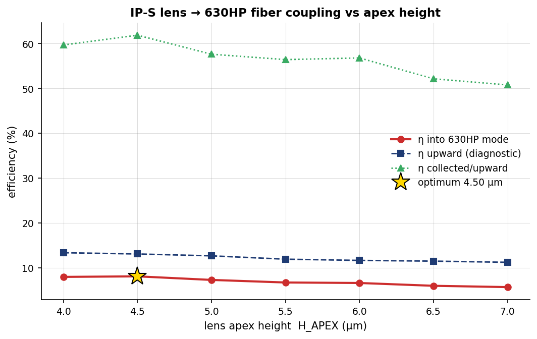 Coupling into the real 630HP LP01 mode vs apex height. Optimum at H_APEX = 4.5 µm
(η = 8.1 %); the curve is shallow.
Coupling into the real 630HP LP01 mode vs apex height. Optimum at H_APEX = 4.5 µm
(η = 8.1 %); the curve is shallow.
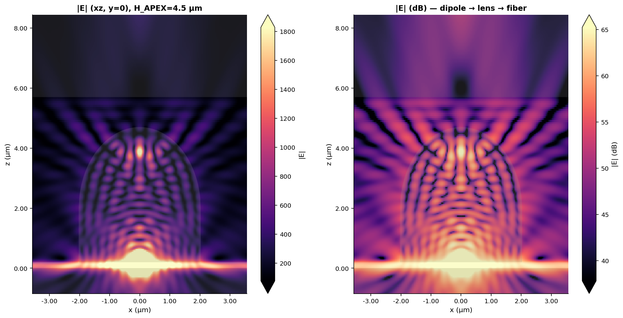 Steady-state |E| at the frozen lens (H_APEX = 4.5 µm), xz plane. Left: linear; right: dB.
The dipole near-field at z ≈ 0.1 µm, the upward beam shaped by the IP-S oval (apex z ≈ 4.7 µm),
and the weak field coupled into the fiber above z ≈ 5.7 µm. The strong lateral spreading at the
emitter plane is the no-mirror loss that Stage 2 recovers.
Steady-state |E| at the frozen lens (H_APEX = 4.5 µm), xz plane. Left: linear; right: dB.
The dipole near-field at z ≈ 0.1 µm, the upward beam shaped by the IP-S oval (apex z ≈ 4.7 µm),
and the weak field coupled into the fiber above z ≈ 5.7 µm. The strong lateral spreading at the
emitter plane is the no-mirror loss that Stage 2 recovers.
Reading the result. The lens captures ~62 % of the upward light into the fiber mode at the optimum — the lens itself is doing its job well. The device-level number (8.1 %) is held down by η_up ≈ 13 %: with no mirror, roughly half the emission goes down into the substrate, and the 57° escape cone plus the mid-plane emitter limit the upward share. That loss is exactly what Stage 2 fixes — the PEC mirror reflects the downward half back up, and the TiO2 cavity adds Purcell directionality. The lens optimum is also nearly flat, so it is robust to the small geometry changes Stage 2 will introduce. Lens frozen at H_APEX = 4.5 µm (aperture ρ_max = 2.03 µm).
3.5 Stage 1b — adding the PEC mirror (cavity sweep, ≈ 2.1 FC)¶
8.1 % is collection-limited: with no mirror, ~half the emission goes down and η_up is only 13 %. The fix is the part of the real stack we had deliberately omitted — the gold mirror (modelled as PEC to cut cost). We added it and ran a 3-knob coordinate-descent sweep:
- SiO₂ spacer thickness (emitter↔mirror distance) — a Drexhage antinode effect,
- lens apex height H_APEX,
- fiber↔lens gap.
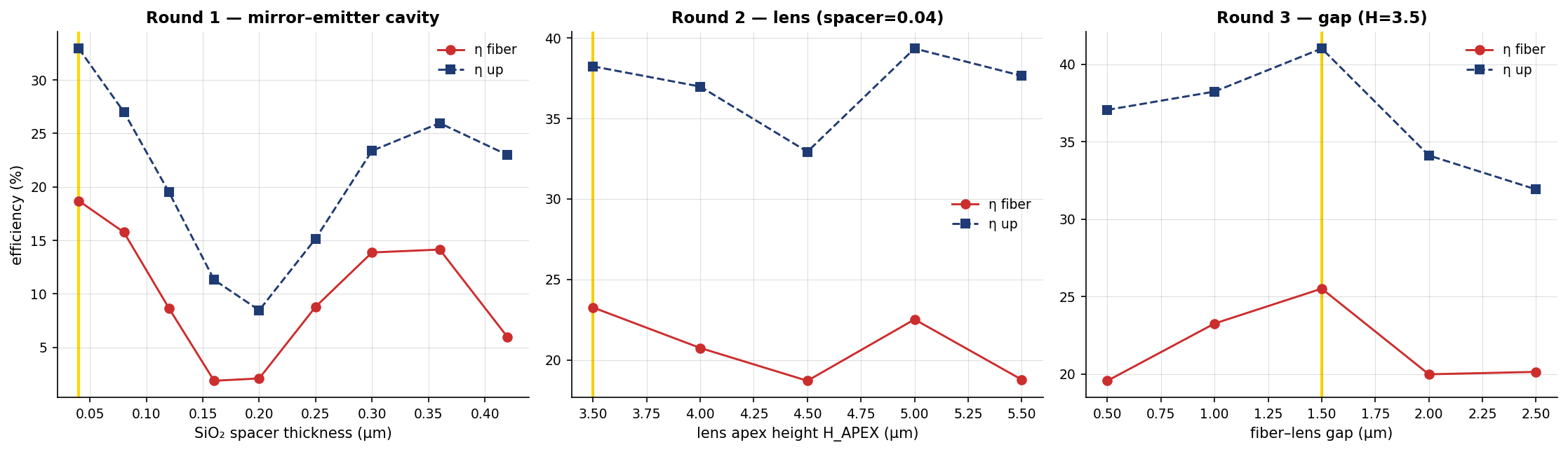 Three-round coordinate descent. Round 1 shows the classic mirror interference: a strong first
antinode at a thin spacer, a null near 0.16–0.20 µm, a weaker second antinode near 0.30–0.36 µm.
Round 2: with the more directional mirror emission a smaller lens (H_APEX ≈ 3.5 µm) is best.
Round 3: a clean interior optimum at gap ≈ 1.5 µm. Gold lines = chosen value.
Three-round coordinate descent. Round 1 shows the classic mirror interference: a strong first
antinode at a thin spacer, a null near 0.16–0.20 µm, a weaker second antinode near 0.30–0.36 µm.
Round 2: with the more directional mirror emission a smaller lens (H_APEX ≈ 3.5 µm) is best.
Round 3: a clean interior optimum at gap ≈ 1.5 µm. Gold lines = chosen value.
| Round | Knob | Range | Optimum |
|---|---|---|---|
| 1 | SiO₂ spacer | 0.04–0.42 µm | 0.04 µm (first antinode) |
| 2 | H_APEX | 3.5–5.5 µm | 3.5 µm |
| 3 | fiber–lens gap | 0.5–2.5 µm | 1.5 µm |
Result at the optimum: η_fiber = 25.5 %, η_up = 41.0 % (lens still captures 62 % of upward) — a 3.1× improvement over the no-mirror 8.1 %.
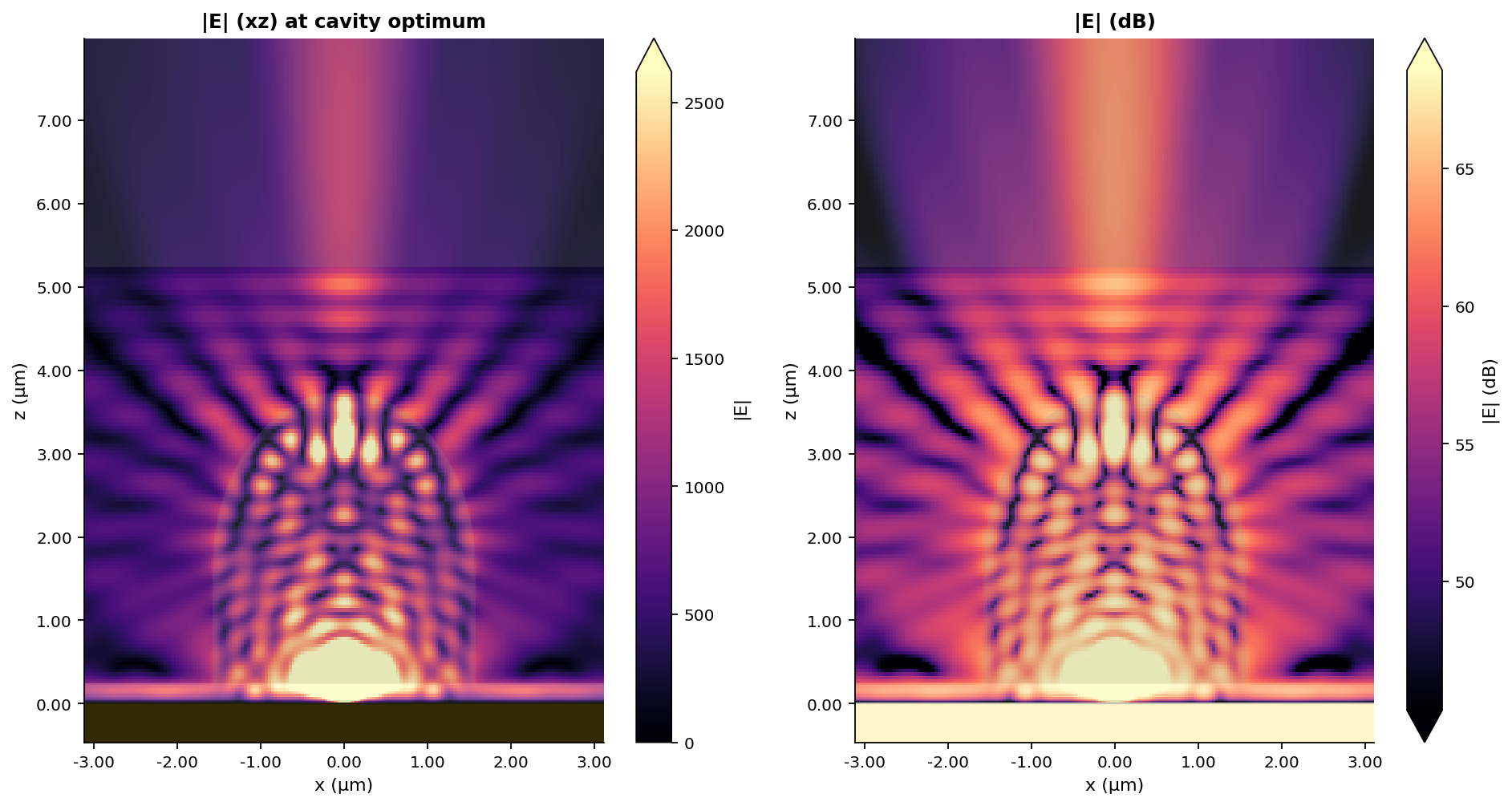 |E| (linear, left; dB, right) at the cavity optimum. Compare with §3.4: the mirror converts
the lateral/downward spray into a directional upward beam that couples cleanly into the fiber.
|E| (linear, left; dB, right) at the cavity optimum. Compare with §3.4: the mirror converts
the lateral/downward spray into a directional upward beam that couples cleanly into the fiber.
Note. The sweep above used a bare crystal (no TiO₂). The real device has a TiO₂ film in the mirror–emitter gap during the Stage-2 optimization, so the spacer must be tuned with that film — see §3.6.
3.6 Stage 1c — spacer optimum WITH the TiO₂ film present (≈ 1.3 FC)¶
The §3.5 sweep omitted the TiO₂. Because the inverse design runs with a TiO₂ film already in the mirror–emitter gap, the spacer must be re-optimised with a uniform 150 nm TiO₂ film (n = 2.4) between the SiO₂ spacer and the crystal. The high-index film is part of the cavity and shifts the antinode. Stack: PEC → SiO₂ spacer (swept) → TiO₂ 150 nm → crystal (emitter mid-plane) → IP-S lens (H_APEX 3.5) → 1.5 µm gap → 630HP fiber.
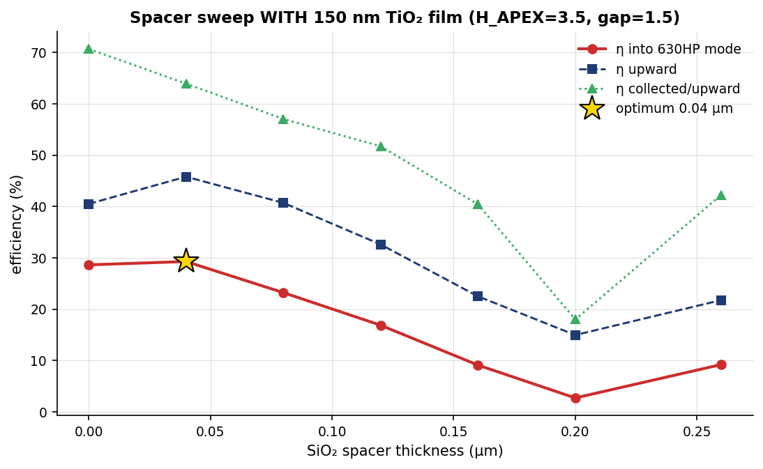 Spacer sweep with the 150 nm TiO₂ film present. First antinode peaks at ≈ 0.04 µm; null near
0.20 µm; second antinode rising past 0.26 µm.
Spacer sweep with the 150 nm TiO₂ film present. First antinode peaks at ≈ 0.04 µm; null near
0.20 µm; second antinode rising past 0.26 µm.
| SiO₂ spacer (µm) | η_fiber | η_up | η collected/up |
|---|---|---|---|
| 0.00 | 28.6 % | 40.5 % | 70.7 % |
| 0.04 | 29.3 % | 45.8 % | 63.9 % |
| 0.08 | 23.2 % | 40.7 % | 57.0 % |
| 0.12 | 16.9 % | 32.6 % | 51.7 % |
| 0.16 | 9.1 % | 22.5 % | 40.4 % |
| 0.20 | 2.7 % | 14.9 % | 18.0 % |
| 0.26 | 9.2 % | 21.8 % | 42.3 % |
With the TiO₂ film, the optimal SiO₂ spacer is ≈ 0.04 µm → η_fiber = 29.3 %, η_up = 45.8 % — higher than the no-film result (25.5 %), because the high-index film reinforces the vertical cavity. This is the passive-stack baseline the Stage-2 inverse design starts from; patterning the TiO₂ (and a true Purcell factor F_P > 1, currently folded into η_up) is the remaining headroom.
Process note (full transparency). Two of the nine spacer points (0.32, 0.40 µm — the second antinode) were not run: a
--spacer --costcommand unintentionally launched the sweep, which was stopped after 7 points (~1.3 FC). The optimum (first antinode at 0.04 µm) is unaffected. The CLI was fixed so--costcan never trigger a run.
Frozen passive cavity for Stage 2: spacer 0.04 µm, TiO₂ 150 nm (to be patterned), H_APEX 3.5 µm, gap 1.5 µm.
4. The full objective: α(F_P)·η (for the later TiO2 inverse design)¶
Once the lens is frozen, the TiO2 inverse-design structure (on the gold mirror + SiO2 spacer, under the crystal) is optimised to maximise the useful single-photon collection:
FOM = α(F_P) · η_collect
4.1 Purcell → effective ZPL branching¶
The intrinsic branching into the zero-phonon line is α₀ = ⅓ (Franck–Condon × Debye–Waller). A Purcell factor F_P enhances only the resonant ZPL rate; the phonon sideband and non-radiative channels (fraction 1−α₀) are unchanged. Hence
α(F_P) = F_P·α₀ / ( F_P·α₀ + (1−α₀) )
where F_P is the total ZPL emission-rate enhancement measured in FDTD (P_emitted / P_emitted,bulk-crystal).
| F_P (total) | α(F_P) | (your convention F = F_P−1) |
|---|---|---|
| 1 | 0.333 | 0 |
| 2 | 0.500 | 1 |
| 5 | 0.714 | 4 |
| 10 | 0.833 | 9 |
| 20 | 0.909 | 19 |
| 40 | 0.952 | 39 |
Note on convention: your example "Purcell factor 10 → α ≈ 0.846" uses (F+1) with F=10, i.e. a total enhancement of 11. In the table above that is the F_P = 11 row. The formula is identical; only the label on the number differs. We will report F_P (total) and state it explicitly so there is no ambiguity.
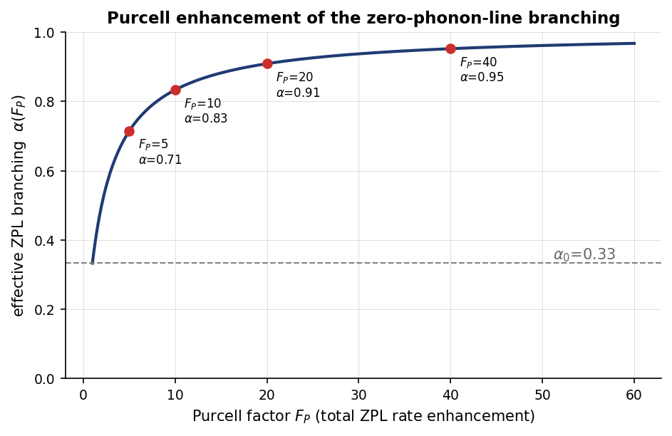 Effective ZPL branching α as a function of the total Purcell factor F_P (α₀ = ⅓).
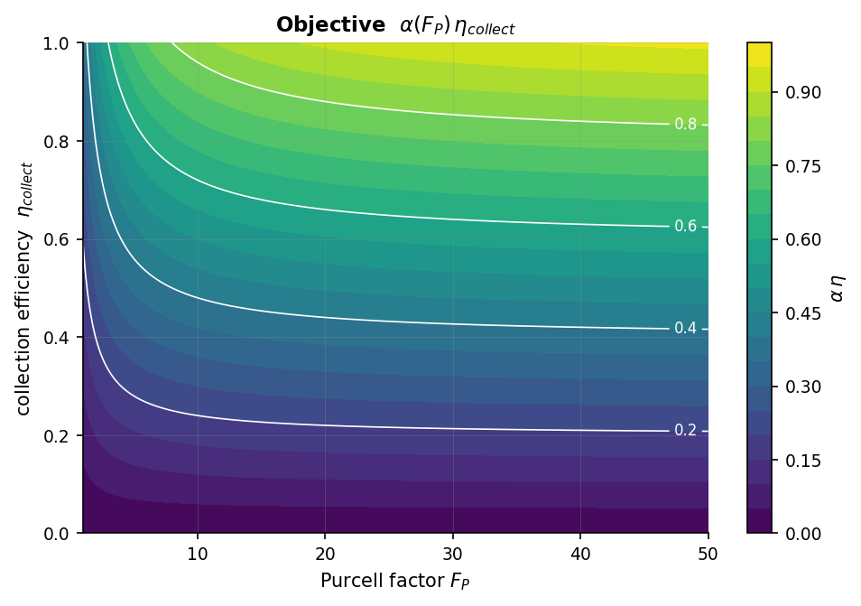 The objective α(F_P)·η over the (F_P, η) plane. Both a high Purcell factor and high collection
efficiency are needed; the inverse design trades them off automatically.
The objective α(F_P)·η over the (F_P, η) plane. Both a high Purcell factor and high collection
efficiency are needed; the inverse design trades them off automatically.
4.2 Differentiable dipole power — six flux planes¶
For the autograd/adjoint inverse design, the denominator P_emitted must be assembled from
six individual planar flux monitors forming a closed box around the dipole, not a
single FluxMonitor box — the box's internal reduction is not differentiable through the
adjoint. F_P is then this 6-plane sum divided by the bulk-crystal reference (one cheap
reference sim of the dipole in homogeneous n=1.8). η_collect uses the fiber ModeMonitor
amplitude. Both numerator and denominator are differentiable, so the full FOM α(F_P)·η is.
4.3 Rough cost outlook for the TiO2 optimization (to be refined)¶
The TiO2 inverse design adds the dispersive gold mirror and a pixelated design region, so a single forward sim will cost more than the lens sweep (rough guess 0.15–0.4 FC). Each optimization step needs a forward + an adjoint sim (~2×). A typical 40–60 step β-annealed run is therefore order 12–40 FC. This is the number we will drive down together — by shrinking the domain, lowering the design-region resolution, using fewer/aliased steps, and a PEC mirror proxy where acceptable — before any optimization is launched. A precise estimate comes with the Stage-2 geometry.
5. Assumptions & open questions¶
- Dipole orientation taken as in-plane (Ey). Anthracene/DBT transition dipoles are in-plane; please confirm the crystal orientation so we fix the axis.
- IP-S index n = 1.51 @ 780 nm (literature ~1.50–1.51). Swappable in one place.
- TiO2 index n = 2.40 (amorphous/anatase sputtered ~2.4). To confirm against your deposition.
- Etched-gap fill of the TiO2 design region assumed to be the spacer oxide (ε_min = 1.45²). Confirm whether gaps are air, oxide, or back-filled by the crystal.
- Spacer / TiO2 thicknesses (150 nm each) are placeholders; they become design variables / knobs in Stage 2.
- The lens-shape sweep deliberately omits the mirror and TiO2 so the lens optimum is not biased by an as-yet-undesigned cavity.
6. What's next (Stage 2 — no credits without approval)¶
- ✅ Lens sweep done (~0.78 FC). Lens frozen at H_APEX = 4.5 µm.
- Build the Stage-2 TiO2 inverse-design geometry: PEC mirror + SiO2 spacer +
pixelated TiO2 design region (air-filled gaps, ε ∈ [1.0², 2.40²]) + crystal + the
frozen lens + 630HP fiber. FOM = α(F_P)·η with the 6-plane differentiable Purcell
and the fiber
ModeMonitor. I'll return a dry-run report with a precise per-step and full-optimization FlexCredit estimate for you to approve before anything runs.
Reproduce this stage: python lens/escape_cone.py · python lens/lens_design.py --cost ·
python lens/run_sweep.py
Results¶
Stage 2 -- TiO2 inverse-design lens results¶
v2 Stage 2 — TiO₂ Inverse Design: Results¶
Adjoint optimization of the TiO₂ cavity layer for α(F_P)·η into 630HP Date: 2026-06-07 · Status: RUN — converged, binarized, verified
1. Result¶
The TiO₂ layer in the mirror cavity was inverse-designed (tidy3d autograd adjoint, 25 β-annealed steps, FOM = α(F_P)·η). The optimizer converged to a concentric-ring (zone-plate-like) TiO₂ pattern that both redirects the emission upward into the lens/fiber mode and enhances the emission rate.
| Design | η (collection) | F_P (Purcell) | α(F_P) | FOM = α·η |
|---|---|---|---|---|
| As-optimized (β = 40) | 56.0 % | 1.88 | 0.484 | 0.271 |
| Hard-binarized (52 % TiO₂ fill) | 54.2 % | 1.93 | 0.492 | 0.266 |
Binarization (the fabricable, fully two-level pattern) costs only 1.7 % of the FOM — the design is robust.
Where this sits in the v2 progression¶
| Stage | η into 630HP | F_P | FOM = α·η |
|---|---|---|---|
| Lens only, no mirror | 8.1 % | 1 (n/a) | 0.027 |
| Passive mirror cavity + uniform TiO₂ film | 29.3 % | (folded in) | ≈ 0.098 |
| Inverse-designed TiO₂ (binarized) | 54.2 % | 1.93 | 0.266 |
The inverse design nearly doubles the collection of the passive cavity (29 % → 54 %) and adds a measured Purcell factor of 1.93, which lifts the zero-phonon-line branching from α₀ = 0.333 to α = 0.49. Net useful single-photon collection α·η ≈ 0.27 — a ~10× improvement over the bare lens.
2. The optimized pattern¶
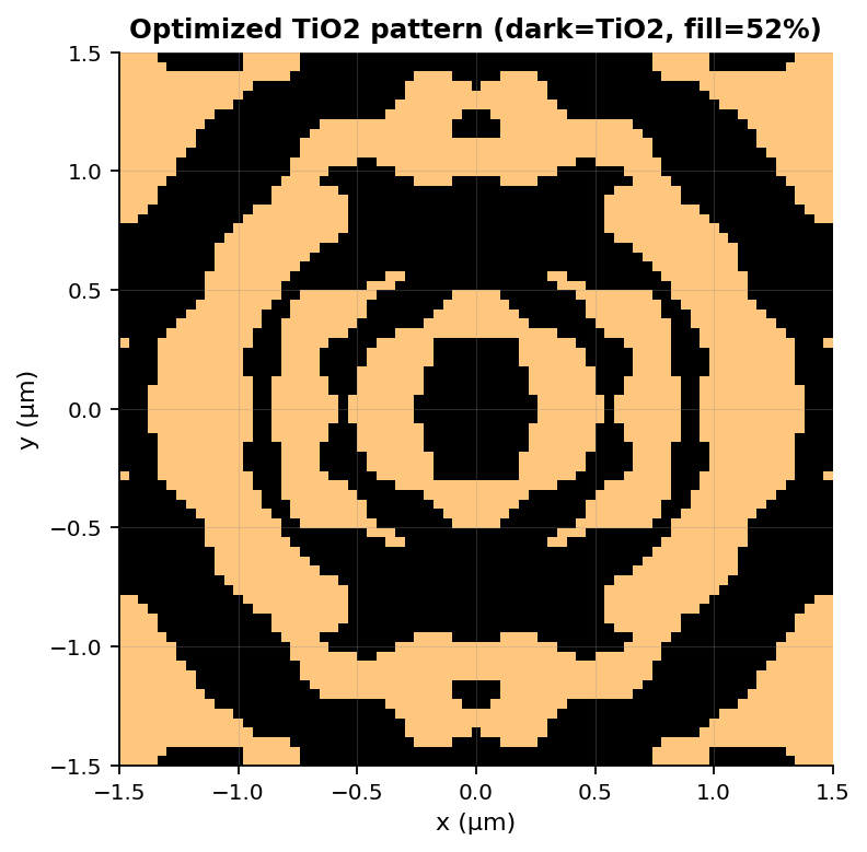 Binarized TiO₂ layer (dark = TiO₂ n=2.4, light = air), 3×3 µm, 52 % fill, 4-fold symmetric.
A central LDOS-tuning feature surrounded by concentric rings — a circular grating / zone plate
that couples the dipole's in-plane and downward emission into the upward fiber mode.
Binarized TiO₂ layer (dark = TiO₂ n=2.4, light = air), 3×3 µm, 52 % fill, 4-fold symmetric.
A central LDOS-tuning feature surrounded by concentric rings — a circular grating / zone plate
that couples the dipole's in-plane and downward emission into the upward fiber mode.
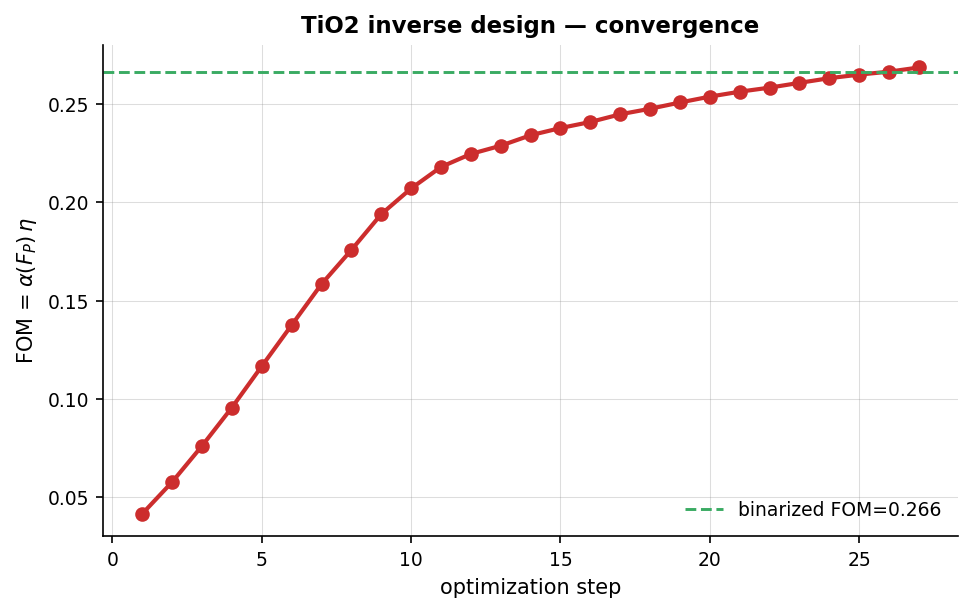 FOM vs optimization step (β annealed 1→40). Smooth, monotonic rise to a plateau; the dashed
line is the binarized design's FOM, essentially on the converged curve.
FOM vs optimization step (β annealed 1→40). Smooth, monotonic rise to a plateau; the dashed
line is the binarized design's FOM, essentially on the converged curve.
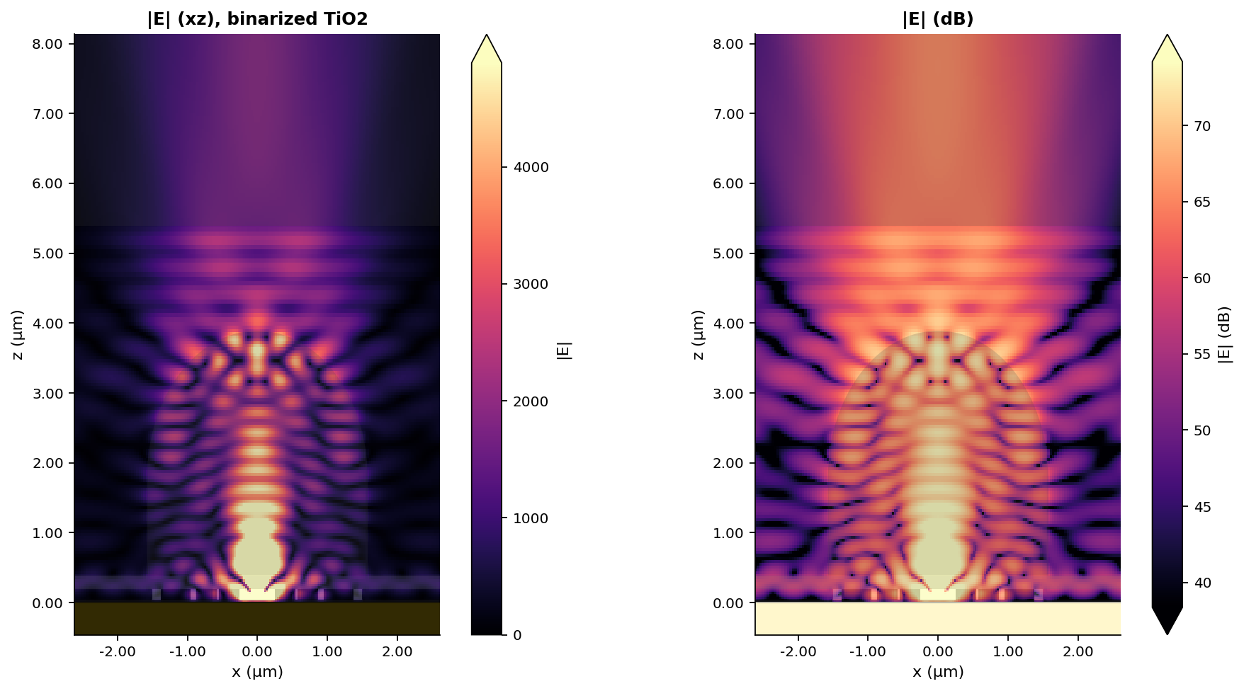 |E| (linear, left; dB, right) for the binarized design. A strong, directional upward beam fills
the lens and couples into the fiber — visibly cleaner and brighter than the passive cavity field.
|E| (linear, left; dB, right) for the binarized design. A strong, directional upward beam fills
the lens and couples into the fiber — visibly cleaner and brighter than the passive cavity field.
3. Method (as run)¶
- FOM = α(F_P)·η, α(F_P) = F_P·α₀/(F_P·α₀+(1−α₀)), α₀ = ⅓.
- η = P(630HP LP01)/P_emit via fiber
ModeMonitoramplitude. - P_emit = Σ six planar FIELD monitors around the dipole (a closed flux box and a
FluxMonitorare not adjoint-differentiable in tidy3d;FieldData.fluxon aFieldMonitoris — that was the key fix). - F_P = P_emit / P_bulk, P_bulk = same dipole in homogeneous crystal (reference sim, 1.848×10⁴).
- Design region 3×3 µm, 40 nm pixels, 100 nm conic-filter min feature, x/y mirror symmetry (~1406 free params), ε ∈ [1.0, 5.76] (air ↔ TiO₂), Adam lr 0.03, β 1→40 over 30 steps.
- Frozen from Stage 1: PEC mirror, 40 nm SiO₂ spacer, 150 nm TiO₂ thickness, crystal + Ey dipole at mid-plane, IP-S lens H_APEX 3.5 µm, 1.5 µm air gap, 630HP fiber.
Run notes. The run is robust but the cloud connection dropped twice (steps 15 and 25); resume + retry logic was added, and the optimization had plateaued by step 25 (last 5 steps gained < 0.01 FOM total), so it was finalized there. Total Stage-2 spend ≈ 4.9 FC.
4. Caveats / next steps¶
- PEC mirror is an idealization; real gold adds ~2–4 % absorption. A single validation sim with dispersive Au should be run before freezing.
- run_time 5 ps appeared sufficient (FOM stable, fields decayed in the plots); a dispersive-Au / higher-Q check should re-confirm.
- The 25/30 steps were enough for convergence; a fully fresh 60-step run from a better start might gain a little, but the current design is already strong and fabricable.
- Could re-open H_APEX / gap / spacer jointly with the pattern for a final polish (cheap).
- Toward fabrication: export the binary TiO₂ pattern to GDS (it's already on the 40 nm grid, 100 nm min feature), then integrate with the rest of the v2 device.
Reproduce: python lens/tio2_inverse_design.py --run 30 then python lens/tio2_finalize.py
Stage 3 -- dual-decoupled lens results¶
v2 Stage 3 — Dual-Port Inverse Design: Results¶
Side-excite (Si₃N₄ waveguide) / top-collect (IP-S asphere → 630HP), decoupled FOM Date: 2026-06-09 · Status: optimization complete; full-lens cross-check pending (network drop)
1. Result¶
A Si₃N₄ partial-etch device layer was inverse-designed (30 β-annealed adjoint steps) to maximise α(F_P)·η_top·min(β_wg/β_min, 1) — bright top collection with a usable waveguide excitation port. Top collection (the frozen asphere) was decoupled from the loop via a mode-overlap against the back-propagated fiber mode (≈ 12× cheaper than putting the lens in the loop).
| Metric | Un-optimized | Optimized |
|---|---|---|
| η_top (collection into 630HP) | ~7.5 % | 23.5 % |
| F_P (Purcell) | ~1.0 | 1.06 (α = 0.347) |
| β_wg (excitation port) | — | 8.7 % (≫ 2 % floor) |
| FOM = α·η_top·clip | — | 0.082 |
The inverse design ~tripled top collection (7.5 → 23.5 %) while keeping the through-bus a usable side-excitation port. F_P stayed ~1: with this FOM, collection is the dominant lever, so the optimizer spent its freedom on directing emission upward rather than on Purcell.
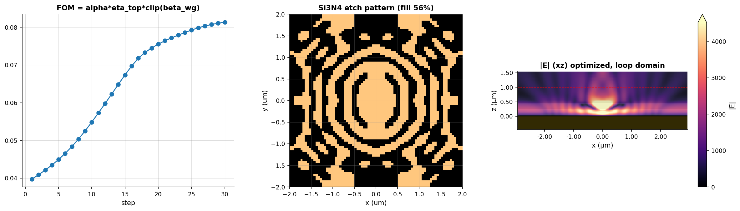 Left: FOM convergence (0.040 → 0.081). Middle: the optimized Si₃N₄ etch pattern — a concentric
circular grating ("bullseye") around the molecule with the through-bus across the centre; 56 %
fill, x/y symmetric. Right: |E| (loop domain) showing the directed upward beam; red dashed = the
near-field overlap plane.
Left: FOM convergence (0.040 → 0.081). Middle: the optimized Si₃N₄ etch pattern — a concentric
circular grating ("bullseye") around the molecule with the through-bus across the centre; 56 %
fill, x/y symmetric. Right: |E| (loop domain) showing the directed upward beam; red dashed = the
near-field overlap plane.
2. Method notes¶
- Decoupled overlap FOM (
dual/dual_decoupled.py): η_top = |⟨E_up, E_target⟩|²/(4P_t)/P_total, with E_target = the 630HP mode launched −z through the asphere and recorded at z_nf = 1.0 µm. Loop domain 5.8 × 5.2 × 1.9 µm (3.9 M cells, x+y symmetry) vs the 19 M-cell full-lens domain. - Sign subtlety (fixed): the target propagates −z; the +z collection mode has the opposite transverse-H sign (E_m, H_m) = (E_t, −H_t). The first run missed this → FOM ≡ 0 and no optimization; the end-of-run full-lens check caught it. After the fix the decoupled η_top reproduced the full-lens value (7.06 % vs 7.51 % on a test design).
- Geometry: PEC mirror · 40 nm SiO₂ · Si₃N₄ (100 nm base + 120 nm etch design, 4 × 4 µm, 180 nm min feature) · through-bus at y = 0 with an x = 0 symmetry plane · crystal + Ey molecule at mid-plane · standard-asphere IP-S lens (R = 1.873 µm, k = −0.439, aperture 2.5 µm) · 630HP fiber. β_wg from the +x waveguide mode (= −x by symmetry).
3. Outstanding¶
- Full-lens cross-check on the optimized design did not run — the cloud connection dropped
immediately after the optimization + decoupled final sim. This is the one remaining validation
(true fiber-
ModeMonitorη_top vs the decoupled 23.5 %); it needs one full-lens sim (~0.3 FC) and awaits explicit approval. - F_P ≈ 1 suggests headroom if Purcell matters: a Purcell-weighted FOM, or a thinner spacer / resonant cavity, could trade some collection for rate enhancement.
Reproduce: python dual/dual_decoupled.py --run 30 (target reused if present)
Downloads¶
Active R&D notebooks only -- no GDS/STL deliverable files exist yet in this tree.
Source: nanophotonic_devices/fiber_collection_optics/v2_lens_codesign/