Splitter + fiber-coupling lenses (v3)
Gen 3: chip+wafer GDS (8 waveguides, Y-junction splitters, KOH v-grooves, Stark electrodes), FDTD-verified splitter (2.37dB excess loss), and a ray-traced two-lens 2PP relay to 630HP fiber.
This directory holds the GDS mask layout for device v3's Si3N4 waveguide
chip: 8 parallel waveguide devices per 10 mm x 10 mm die, each running
facet -> short propagation -> 50:50 Y-junction splitter -> two branch
waveguides -> KOH v-groove fiber coupling, plus the Stark-tuning electrodes
and both alignment-mark systems. See
device_architectures/v3/README.md (repo root)
for the full device architecture (molecule-in-cavity Stark-tuning geometry,
silver-mirror variant, wafer stack) that this layout implements.
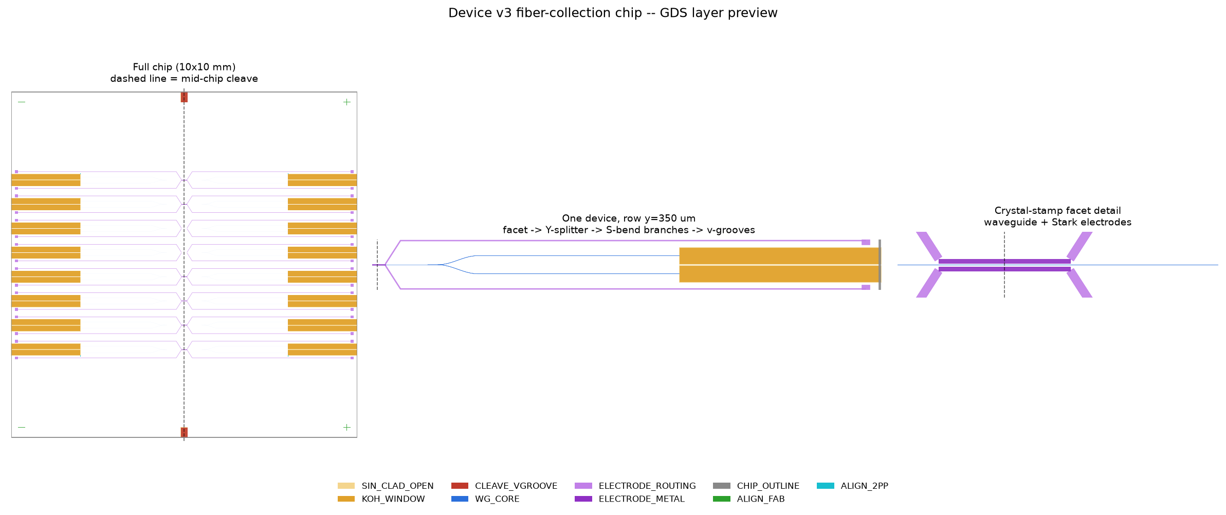
Full 10x10 mm chip (left), one device's facet-to-v-groove path (center), and the crystal-stamp facet detail: waveguide + Stark electrodes (right).
Generated by build_v3_gds.py (gdstk 1.0.1, .venv/bin/python).
Run it from the repo root:
It writes chip.gds, wafer.gds, and figures/schematic.png.
Downloads
- GDS:
chip.gds(single 10x10 mm die, 16 devices) --wafer.gds(4-inch wafer, 60 dies) - STL (2PP lens print files, see "Fiber-coupling lens design" below):
lens1_waveguide_facet.stl,lens2_fiber_tip.stl,lens1_support_ring.stl
This is a layout/design deliverable, not a simulation: dimensions below are either taken directly from the PI's spec, taken from real fab-process geometry (the 54.74 degree KOH etch angle), reused from this repo's own FDTD/mode-solve work where it already exists (waveguide width, see below), or a stated engineering judgment call. Nothing here is a simulated or measured result.
How this connects to the rest of device v3
- Waveguide width (0.4 um) is taken directly from
splitter_fdtd/splitter_sim.py, a parallel FDTD study in this same directory that verified a 0.4 um wide, 300 nm thick Si3N4 strip is single-mode at 780 nm and sized its own Y-junction stem to 0.9 um. This GDS's Y-junction taper is sized to the same 0.9 um stem (2*WG_WIDTH + JUNCTION_GAP = 0.9 um) so the two designs describe the same physical waveguide, even though the FDTD study only needs a ~10 um unit cell and this GDS lays out the full chip-scale splitter, S-bend, and v-groove pitch. - Fiber mode target (125 um cladding, ~5 um MFD) matches the fiber
numbers used in
fiber_lens_raytrace.py(this directory) and indbt_tir_sil_fiber_coupler_v1/v2_lens_codesign, run by a parallel workstream doing the 2PP aspheric lens ray-trace design and STL export for the same v-grooves this GDS lays out. That script'sstl/outputs (lens1_waveguide_facet.stl,lens2_fiber_tip.stl, a support ring) are meant to be printed at the two facet locations this layout defines: the waveguide's second (fiber-coupling) facet atx = FACET2_Xand the fiber tip seated in the v-groove. This GDS does not attempt to draw the lenses themselves — only theALIGN_2PPmarks the 2PP printer needs to find those facets. - Molecule/Stark-tuning geometry (crystal stamp, Ag mirror, electrode
cross-section) is specified in
device_architectures/v3/README.md(repo root) and studied at the field level inelectronics_electrostatics/v3_stark_tuningandnanophotonic_devices/emitter_coupling/anthracene_facet_mirror_coupling_v3. This GDS only lays out the electrode metal footprint and its routing — it does not compute the resulting Stark field.
Top-level geometry: mirror-symmetric about the mid-chip cleave
The spec says the chip is cleaved down the middle, perpendicular to the
waveguides, to expose the crystal-stamp facet, and that a crystal is
stamped onto one exposed facet per device. The cleanest way to satisfy
both of those statements at once — and the one this layout uses — is to
make the whole 10 mm chip mirror-symmetric about the cleave line
(x = 0): every one of the 8 waveguide rows is actually built twice, once
for x > 0 and once for x < 0, as mirror images of each other. Cleaving
at x = 0 then splits the single 10 mm x 10 mm mother chip into two
independent 5 mm x 10 mm devices, each with its own freshly-cleaved facet
at the former mid-line (where its crystal gets stamped) and its own splitter
+ branches + v-grooves running out to the die's original outer edge (where
the fiber enters from outside). This doubles device yield per lithography
run and is why the chip is specified as 10 mm long in the first place
rather than 5 mm. chip.gds therefore contains 16 physical waveguide
devices (8 rows x 2 mirrored halves), which become 2x8 = 16 separate
devices once cleaved and diced.
The full path per device, x measured outward from the cleave facet:
| segment | x range (um) | length (um) |
|---|---|---|
| facet -> Y-junction start (propagation) | 0 - 500 | 500 |
| Y-junction adiabatic taper | 500 - 600 | 100 |
| S-bend to full branch separation | 600 - 1000 | 400 |
| straight branch to 2nd facet | 1000 - 3000 | 2000 |
| KOH v-groove / fiber facet | 3000 - 5000 | 2000 |
Parameter choices and rationale
Waveguide count and pitch. 8 waveguides (within the 5-10 spec range) on a 700 um pitch. This is well beyond any crosstalk floor (the repo's own rule of thumb, >=20-50x core width for weakly-guiding Si3N4/SiO2 at ~780 nm, would only require ~8-20 um at a 0.4 um core width — 700 um is ~1750x that). The pitch is actually set by a fab/layout constraint, not crosstalk: each row's KOH v-groove window (160 um wide, see below) and its independent, single-metal-layer Stark-electrode routing corridor (out to its own bond pad near the outer edge, see "Electrode routing" below) both have to fit inside one row's own half-pitch without touching the neighboring row's v-groove. 8 rows x 700 um = 4900 um total array width, comfortably inside the 10 mm chip with room left over for alignment marks and the cleave-guide notches.
Waveguide width, 0.4 um. Reused from splitter_fdtd/splitter_sim.py's
FDTD-verified single-mode Si3N4 strip at 780 nm / 300 nm film thickness (see
"How this connects" above) rather than re-guessed here.
Propagation length before the splitter, 500 um. Per the spec ("a few hundred um to low-single-digit mm"): long enough that the mode has settled away from the facet and the cleave-guide notch before it hits the junction, short enough that propagation loss is a non-issue for Si3N4 (a typical Si3N4/SiO2 strip loses well under 1 dB/cm, so 500 um = 0.05 cm costs a small fraction of a dB — not simulated here, just noted as the reason the number doesn't need to be tightly optimized).
Splitter type: Y-junction, not a directional coupler. An adiabatic
Y-junction was chosen because it is broadband and comparatively tolerant of
fabrication error (splitting ratio depends on the taper geometry, not on
hitting a precise few-hundred-nm coupling gap over a precise coupling
length, the way a directional coupler's 50:50 ratio does). That fab
tolerance matters more here than the extra chip real estate a Y-junction
costs, since this is a first-generation device. splitter_fdtd/splitter_sim.py
verifies this choice at the FDTD level; this GDS just lays out the same
topology at chip scale (taper to a 0.9 um stem, then a raised-cosine S-bend
out to a 180 um branch separation).
Branch separation and KOH window width (fiber v-groove sizing). Branch centerlines end up ±90 um from the row centerline (180 um separation) — comfortably more than a 125 um bare-fiber cladding diameter, leaving ~55 um of clearance between the two fiber surfaces. The KOH mask-opening width per groove is 160 um; see the KOH v-groove geometry section below for why.
Cleave-guide notches. Two small (200 um wide x 300 um deep) windows on
the CLEAVE_VGROOVE layer, cut into the top and bottom chip edges exactly
at x = 0, opened through the dielectric stack the same way as the fiber
v-grooves (same KOH step). These are stress-riser notches to make the
mid-chip cleave track a straight line through the whole array rather than
wander — a standard technique, not a fiber-holding groove.
KOH v-groove geometry (54.74 degree <111> sidewalls)
KOH etches Si3N4/SiO2 essentially not at all, so wherever a v-groove is
needed the dielectric stack must first be opened down to bare Si — that
opening is the KOH_WINDOW layer (and CLEAVE_VGROOVE for the
cleave-guide notches, same process step, sibling datatype so mask-house
documentation can tell the two purposes apart). SIN_CLAD_OPEN is the
lithography step that actually removes the Si3N4 + SiO2 (drawn 5 um larger
on each side than KOH_WINDOW/CLEAVE_VGROOVE, a process-margin bias so
the dielectric clears fully around the Si etch window under normal mask
alignment tolerance). Judgment call: I treated SIN_CLAD_OPEN and
KOH_WINDOW as two literal process steps sharing (almost) one footprint —
dielectric dry etch, then Si wet etch — rather than as two unrelated
patterns; please confirm this matches the intended process flow.
For a rectangular mask opening of width W etched anisotropically in
(100) Si with a KOH-style etchant, the sidewalls are the slow-etching
{111} planes at alpha = 54.74 deg from the wafer surface, and the etch is
self-limiting: the two sidewalls meet at a point on the window's centerline
at depth
and — critically — an ideal self-limited V-groove never extends laterally
beyond its own mask window, so adjacent windows with any nonzero silicon
septum between them remain physically separate grooves (this is why
KOH_WINDOW polygons for neighboring branches/rows only need to not
overlap, not maintain some larger minimum spacing; the layout is checked
programmatically to have zero window-to-window overlap).
For a bare fiber of diameter d resting in the groove and touching both
sidewalls (not the apex), the fiber center sits a depth below the mask
plane of
With d = 125 um (standard SMF cladding, matching the fiber target used
in fiber_lens_raytrace.py): depth_to_center = 62.5 / sin(54.74 deg) =
76.55 um. This layout uses W = 160 um, giving a self-limited depth
D = 113.1 um — about 36.6 um deeper than the fiber needs, so the fiber
seats on the sidewalls with clearance above the groove apex rather than
bottoming out. (This groove-width choice also needs to leave room for the
branch separation, see above: 2*BRANCH_OFFSET + W = 340 <= WG_PITCH/2 for
each half-lane's window not to touch the neighboring row's window — checked
programmatically, see "Validation" below.)
Open question for the PI/process engineer: getting the fiber core height
to line up with the 300 nm-thick Si3N4 core (itself sitting atop 4 um of
undercladding oxide) to sub-micron precision is a cross-section/etch-depth
matching problem this 2D mask layout doesn't solve — it only sizes the
groove to seat the fiber mechanically. Also, I assumed the waveguide's
second (fiber-facing) facet is defined by a separate, more standard,
smooth (e.g. dry/RIE) etch step right at the KOH_WINDOW's inner edge,
not by the sloped KOH sidewall itself — a sloped KOH wall would make a
poor optical coupling facet. Please confirm that's the intended process;
if not, this boundary needs to move.
Electrode routing (single metal layer, no crossings)
The Stark-tuning electrodes flank each waveguide in-plane at ±y, right at
the crystal-stamp end (x = 0 to 80 um, 5 um wide metal, 2 um clear of
the waveguide edge). Each electrode needs its own routing trace out to a
bond pad at a chip edge, without shorting to the waveguide, to the other
electrode of the same pair, or to any other row's electrode.
The first design I tried routed all rows' electrodes to shared bond-pad
rows along the chip's top/bottom edges (a bus/fan-out). That topology
necessarily crosses many electrode traces over each other in projection —
solvable in a real process with a second metal layer + vias, but not with
the single ELECTRODE_METAL/ELECTRODE_ROUTING layer this spec asks for.
So instead, each row's routing stays entirely inside that row's own
±350 um half-lane: a short local jog from the electrode out to a
routing corridor 240 um from the row centerline (comfortably outside that
row's own KOH window, which only extends to 90+80 = 170 um), then straight
in +x, parallel to that row's own v-groove, out to a bond pad
(80 x 80 um) 150 um in from the outer edge. Because no row's routing ever
leaves its own lane, no trace can cross another row's waveguide, electrode,
or routing trace — verified programmatically (see "Validation" below), not
just by inspection.
Trade-off worth flagging to the PI: this puts the 16 Stark-electrode bond pads in the same edge region as the 16 fiber v-grooves, which may be a packaging inconvenience during fiber attach. The alternative (bond pads on the top/bottom edges, away from the fiber region) is possible but needs a second metal layer with vias to cross over neighboring waveguide lanes — flagged here as an open question rather than silently built in, since no upper-cladding thickness (needed to isolate a crossing metal trace from the buried SiN core) isn't specified anywhere in the v3 wafer stack.
Alignment marks (two distinct systems, two distinct layers)
ALIGN_FAB— general wafer/stepper fab alignment: a 200 um corner cross at each of the chip's 4 corners (inset 300 um), in the style ofdevice_architectures/v1/gds/electrodes_v1.ipynb'sconstruct_corner_cross.ALIGN_2PP— separate, finer (40 um arm) crosses placed specifically near the fiber-coupling region (near the waveguide's 2nd facet and near the fiber tips, both chip halves), for the 2PP printer that writes the aspheric lenses at those two locations. Kept on its own layer per the spec, since these marks serve a different tool/process step thanALIGN_FABand shouldn't be confused with it.
The silver mirror itself (50 nm Ag, blanket-coated on the second half's facet after cleaving, before re-fusing the two halves) is not drawn on any GDS layer — it's a blanket evaporation, not a lithographically patterned step.
wafer.gds
A 101.6 mm (4-inch) diameter wafer, matching the diameter convention used
in crystal_deposition/hex_dot_wafer_boy_v1/generate_gds.py, tiled with a
10 x 10 grid of 10 mm chips (also matching that project's grid convention).
Unlike that project, which lays out the full 10x10 square grid without
clipping to the physical wafer circle (circular_wafer_clipping: False in
its layout_params.json — deliberate for that project's purposes, since it
wasn't meant to represent a real single-wafer tapeout), wafer.gds here
does clip to the wafer: only chips whose corners fall inside the wafer
radius (minus a 500 um edge-exclusion margin) are placed, giving 60
placed chips — a realistic yield for 10 mm dies on a 100 mm-class wafer.
WAFER_OUTLINE (layer 10) is a ring plus a straight primary flat (SEMI
M1.15-style, 32.5 mm flat length for a 100 mm <100> wafer) computed from
the actual flat-chord geometry, not just an arbitrary notch. WAFER_ALIGN
(layer 11) holds two wafer-level alignment crosses near the flat, distinct
from every chip's own ALIGN_FAB marks.
GDS layer table
| Layer (num, type) | Name | Purpose |
|---|---|---|
| (1, 0) | WG_CORE |
Si3N4 waveguide core: facet->splitter straight, Y-junction taper, both S-bend branches |
| (2, 0) | KOH_WINDOW |
Si3N4+SiO2 opened to bare Si -- fiber-seating v-groove KOH etch mask |
| (2, 1) | CLEAVE_VGROOVE |
Same KOH etch step, cleave-initiation stress-riser notches at the mid-chip cleave line |
| (7, 0) | SIN_CLAD_OPEN |
Dielectric (Si3N4+SiO2) removal mask, 5 um biased vs. KOH_WINDOW/CLEAVE_VGROOVE |
| (3, 0) | ELECTRODE_METAL |
In-plane Stark-tuning electrodes flanking the waveguide, ±y, at the crystal-stamp end |
| (3, 1) | ELECTRODE_ROUTING |
Electrode routing traces + bond pads (same metal, sibling datatype) |
| (4, 0) | ALIGN_FAB |
General wafer/stepper fab alignment marks (chip corners) |
| (5, 0) | ALIGN_2PP |
Fine alignment marks for the 2PP lens printer, near the fiber-coupling region only |
| (6, 0) | CHIP_OUTLINE |
Chip boundary reference frame (not a fab mask layer) |
| (10, 0) | WAFER_OUTLINE |
Wafer edge ring + primary flat (wafer.gds only) |
| (11, 0) | WAFER_ALIGN |
Wafer-level alignment marks, distinct from per-chip ALIGN_FAB (wafer.gds only) |
Validation
build_v3_gds.py only builds the geometry; the checks that it doesn't
short anything together were run separately (not checked into this
directory as a script, since it was a one-off sanity pass, not a reusable
tool) by loading chip.gds back with gdstk and using boolean and/or
ops to confirm, layer by layer: no KOH_WINDOW self-overlap, no
ELECTRODE_METAL self-overlap, no ELECTRODE_ROUTING net-to-net overlap
(grouping each trace with its nearest bond pad), and no unwanted overlap
between WG_CORE/ELECTRODE_METAL/ELECTRODE_ROUTING and KOH_WINDOW.
All passed cleanly. The one expected "violation" is that SIN_CLAD_OPEN
extends 5 um past the nominal x = +/-5000, y = +/-5000 die edge at the
cleave notches and the outer v-groove edge — an artifact of the deliberate
5 um process-margin bias landing exactly on the die boundary, well inside
any real dicing kerf (tens of um), not a real problem.
Open questions / judgment calls for the PI
- Waveguide-to-fiber facet formation: assumed a separate smooth etch defines it, not the sloped KOH wall itself (see KOH section above).
- Stark-electrode bond pads sit near the fiber v-groove region rather than the top/bottom chip edges, to keep routing single-layer and crossing-free (see "Electrode routing" above) — confirm this packaging trade-off is acceptable, or specify an upper-cladding thickness so a second metal layer / over-waveguide crossing can be used instead.
SIN_CLAD_OPENvs.KOH_WINDOWtreated as one physical opening drawn on two layers for two process steps (dielectric etch, then Si etch) — confirm this matches the intended process, and that a 5 um bias is a reasonable process margin.- Waveguide width (0.4 um) and Y-junction stem width (0.9 um) are pulled
from the parallel
splitter_fdtd/splitter_sim.pyFDTD study rather than independently chosen here, so the two deliverables describe the same waveguide — flag if that study's numbers change. - Fiber v-groove length (2000 um) and KOH mask-opening width (160 um) are sized for mechanical seating of a 125 um cladding fiber with margin, not simulated or measured; the KOH window's mask-opening-to-etch-depth formula is real fab physics but the numeric width choice itself is a judgment call.
Fiber-coupling lens design
(This section documents fiber_lens_raytrace.py, a
parallel workstream to the GDS layout above — it designs the two 2PP-printed
aspheric lenses that bridge each waveguide's second facet to its fiber tip.
It shares the same waveguide width (0.4 um) and fiber choice (630HP, 125 um
cladding) as the GDS above; see "How this connects to the rest of device v3"
near the top of this file for the cross-link. Run python fiber_lens_raytrace.py
from this directory to regenerate everything below.)
Approach: two-lens relay, not a single bridging lens
The PI's spec allows either a single lens spanning the free-space gap or a two-lens relay. This design uses two independently-designed single-surface aspheres — one printed on the waveguide facet, one printed on the fiber tip, joined by a collimated free-space beam — because:
- each lens can be exactly solved on its own (collimate a point source / refocus a collimated beam are both closed-form, zero-on-axis-aberration problems for the right conic; a single bridging lens imaging one small, highly-divergent mode straight into a much larger, low-divergence one is not a closed-form single-surface problem),
- it decouples the two very different jobs at the two facets: Lens 1 has to capture a ~47 deg half-angle wide-angle launch from a deeply sub-wavelength waveguide mode; Lens 2 only has to deliver a ~4 deg gentle focus into the fiber's low NA. Forcing one surface to do both is a much harder aberration-correction problem than two purpose-built ones, and
- it matches this repo's own precedent (
solid_immersion_lens/v2..v6'sdual_lens_stl.ipynb/dual_lens_generatorpattern already builds independent lens pairs joined by an air gap).
1. Waveguide mode
Si3N4 (n=2.00) core / SiO2 (n=1.45) under-clad / air top+side-clad strip,
300 nm film thickness (fixed by the v3 wafer stack), 400 nm width —
reused from splitter_fdtd/splitter_sim.py's FDTD-verified single-mode
choice in this same directory (see "How this connects" above), not
re-guessed here.
Mode solved by the effective-index method (1D asymmetric slab in z, then a 1D symmetric slab in y using the vertical neff as the effective core index) at 780 nm:
| quantity | value |
|---|---|
| vertical-slab neff (infinite width) | 1.8209 |
| 2D EIM neff (TE0-like) | 1.6871 |
FDTD reference neff, same 400x300 nm cross-section (anthracene_slab_wg_coupling_v1, TE0) |
1.6720 |
| EIM vs. FDTD difference | +0.90% |
| MFD (horizontal, y) | 437 nm |
| MFD (vertical, z) | 377 nm |
| circularized MFD / waist w0 | 406 nm / 203 nm |
The 0.9% neff agreement against an independent full FDTD mode solve elsewhere in this repo (same waveguide cross-section, different project) is used here as the validation for the analytic EIM approach, per the task's suggestion to reuse/cross-check rather than blindly recompute.
2. Fiber target
630HP, reused as-is from dbt_tir_sil_fiber_coupler_v1 /
v2_lens_codesign for consistency with the rest of this product line:
MFD = 5.0 um (w0 = 2.5 um) at 780 nm, datasheet NA = 0.12, core/clad index
1.462/1.457, 125 um cladding diameter (matches the v-groove sizing in the
GDS section above). Its Gaussian-mode-equivalent divergence half-angle
(5.7 deg) is reasonably close to the datasheet NA's half-angle (6.9 deg) —
expected, since datasheet NA is the larger 1%-power definition, not the
fundamental-mode Gaussian divergence.
3. Lens prescription
Both surfaces use the standard sag equation, sag(r) = c*r^2 / (1 +
sqrt(1 - (1+k)*c^2*r^2)) + A4*r^4, c = 1/R, resin index n = 1.51
(Nanoscribe IP-S, reused from v2_lens_codesign's N_IPS), at 780 nm.
k is fixed at the exact aplanatic (zero on-axis spherical aberration for
a point source / collimated-beam conjugate) value for each interface;
R is solved from Gaussian-beam (complex-q, ABCD) ray-transfer propagation
so the relay's output waist and wavefront exactly match the fiber's
fundamental mode.
| Lens 1 (waveguide facet) | Lens 2 (fiber tip) | |
|---|---|---|
| interface | resin -> air | air -> resin |
| R | 2.030 um | 26.882 um |
| k | -0.4386 (ellipse) | -2.2801 (hyperbola) |
| A4 | 0 | 1.263e-4 um^-3 (ray-trace-optimized, see below) |
| apex height / standoff | h_apex = 6.0 um above the facet | 65 um standoff from Lens 2's flat base to the fiber core plane |
| aperture radius used | 2.71 um (full natural aperture) | 14.8 um (clipped to the beam radius arriving from Lens 1) |
The gap between the two lenses (15 um) and Lens 2's 65 um standoff to the fiber facet are assembly/fabrication design choices, not lens-shape free parameters — flagged for the PI/mechanical design to confirm against the actual post-cleave and v-groove geometry (the GDS section above doesn't yet pin these distances down independently). The 65 um standoff in particular is a real, load-bearing number: it is the low-NA lens's own working distance to reach the target 2.5 um fiber waist, and will need either a printed spacer feature or a v-groove/fiber-holder offset of that size.
4. Predicted performance (honestly caveated)
Geometric ray tracing (exact Snell's law through both surfaces, point source at the waveguide facet) confirms Lens 1 is exactly aplanatic at any angle (by construction) and reveals that Lens 2 — whose radius was matched via paraxial Gaussian propagation, not an exact wide-angle condition — has real residual spherical aberration: 417 nm RMS spot at the fiber plane with a plain conic, reduced to 339 nm RMS (19%) after optimizing a quartic correction term via the ray trace. Off-axis (mode-edge launch, ±203 nm) blur is larger still (~2.1 um RMS) — this is finite-source-size (coma-like) blur that a point-source-designed conic cannot remove by itself. Ray tracing alone cannot turn any of this into a coupling efficiency number (geometric optics has no concept of a diffraction-limited spot size), so:
Predicted coupling efficiency comes from a separate, standard Gaussian-mode-overlap calculation (waist- and wavefront-curvature-matching, the closed-form fiber-coupling-theory formula) using the same lens prescription's paraxial ABCD propagation, times a normal-incidence Fresnel transmission estimate across all four real interfaces (WG core -> resin, resin -> air at Lens 1, air -> resin at Lens 2, resin -> fiber core):
- Gaussian-mode overlap (waist + curvature matched by design): 100% (by construction of the paraxial design — not itself informative beyond confirming the solve converged correctly)
- combined Fresnel transmission (4 interfaces, uncoated, normal-incidence estimate): 91.6%
- combined estimate: ~92%
This number should not be taken as a rigorous prediction. In particular:
- The waveguide mode's circularized waist (203 nm) is only ~0.4x the wavelength-in-resin (520 nm); its Rayleigh range (~0.25 um) is far smaller than the print working distances used here. Both paraxial Gaussian-beam propagation and geometric ray tracing are rough approximations in this near-field regime — a rigorous number needs a full-wave launch (FDTD/BPM/eigenmode expansion), not ray/Gaussian optics.
- The design uses a circularized (rotationally-symmetric) approximation of the waveguide mode, which is actually elliptical (437 nm x 377 nm) — real coupling will have some additional ellipticity-mismatch loss not captured here.
- Fresnel loss is a normal-incidence estimate; Lens 1's rays are launched up to ~47 deg from normal, where the true (angle- and polarization-dependent) transmission is measurably different from the normal-incidence number used.
- No coating is assumed.
What this analysis genuinely establishes, without over-claiming: the lens prescriptions are self-consistent (waist and wavefront exactly matched at the design point), the geometric aberration is small compared to the target fiber spot size (339 nm vs. 2.5 um, ~14%), and the assembly tolerances are asymmetric — see the sensitivity figure below — the relay is comparatively forgiving of gap-length (defocus) error (broad tolerance, consistent with Lens 2's low NA) but sensitive to lateral misalignment between the two lenses (efficiency estimate drops from 100% to ~79% over 0-1.2 um of decenter in the simplified source-offset proxy model used here — flagged in the script as a proxy, not a full independent two-lens decenter analysis).
5. STL files (stl/)
lens1_waveguide_facet.stl— Lens 1, revolved solid, 2.71 um aperture radius, 6.0 um apex height + 1.0 um flat base, ready to print directly on the waveguide's second facet.lens2_fiber_tip.stl— Lens 2, revolved solid, 14.8 um aperture radius, 3.7 um apex height + 1.0 um flat base, ready to print on/near the fiber tip.lens1_support_ring.stl— an annular scaffold stub around Lens 1. Lens 1's steepest flank is only ~3 deg from vertical (well within typical 2PP self-supporting overhang limits), so this is included as a conservative print-anchor/proximity-relief feature rather than a strict structural necessity — Lens 2's flank is even gentler and gets no support structure.
6. Figures (figures/) and data (data/, reports/)
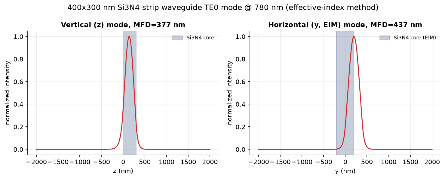
The solved TE0 intensity profile in each transverse direction, with the Si3N4 core region and MFD called out.
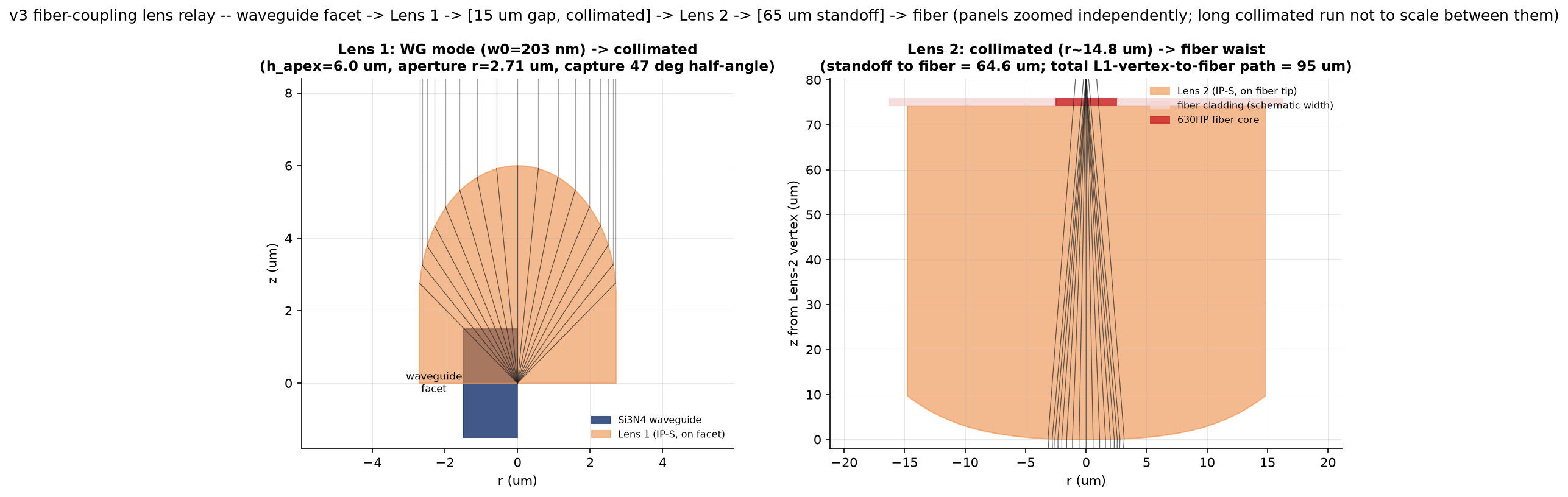
Two-panel ray-fan schematic: Lens 1's wide-angle launch and collimation (left), Lens 2's gentle refocus onto the fiber (right); panels are zoomed independently since the ~65 um standoff run between them would otherwise dwarf both lenses in a single to-scale drawing.
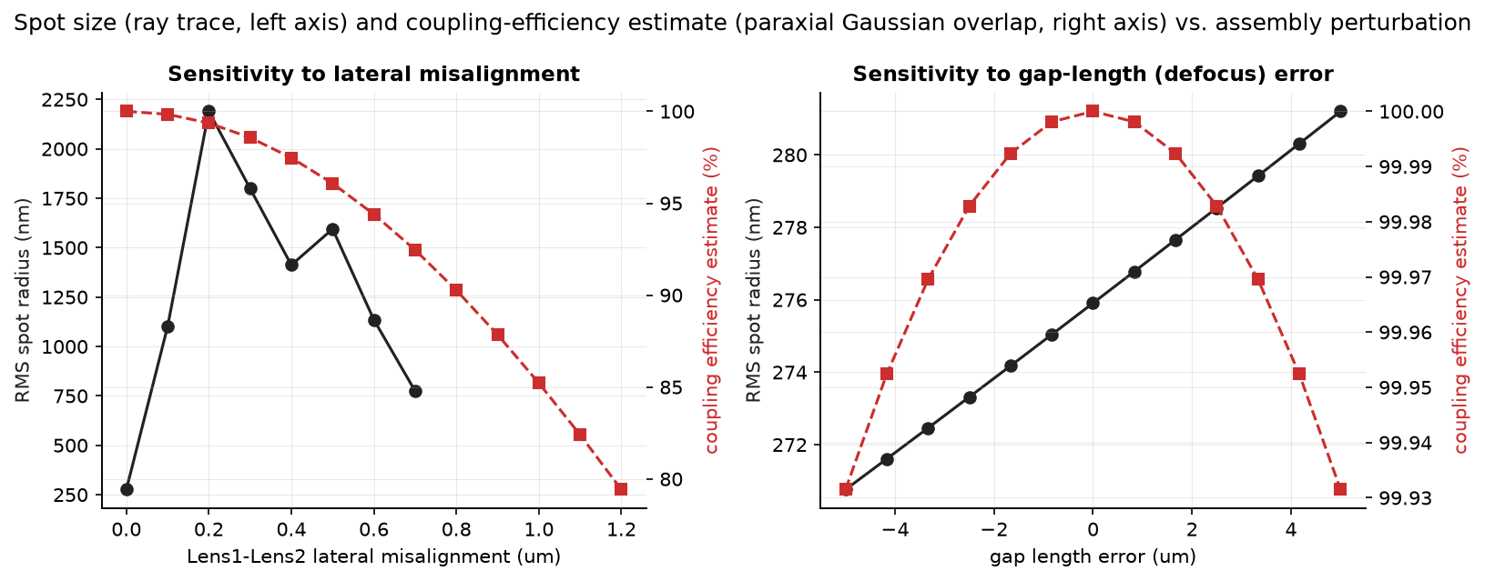
RMS spot size (ray trace) and coupling-efficiency estimate (Gaussian overlap) vs. lateral misalignment and vs. gap-length (defocus) error.
data/results_*.json / reports/report_*.md — full numeric results,
lens prescriptions, and the caveats list above, machine- and
human-readable respectively.
Judgment calls for the PI to sanity-check
- Two-lens relay vs. single bridging lens — chosen for independent solvability and very different NA requirements at the two facets (see above); a single-lens bridge was not attempted.
- Waveguide width (400 nm) — reused from
splitter_fdtd/splitter_sim.pyin this same directory; independently cross-checked here against an existing FDTD mode solve (0.9% neff agreement) rather than re-simulated. - Fiber choice (630HP) — reused from
dbt_tir_sil_fiber_coupler_v1/v2_lens_codesignfor product-line consistency; not re-derived from first principles. - Lens material (IP-S, n=1.51) — assumed, reused from
v2_lens_codesign; not confirmed against a specific resin datasheet for this project. - Gap (15 um) and Lens-2-to-fiber standoff (65 um) — engineering assumptions, not yet coordinated with the GDS/mechanical layout above or with a real post-cleave/v-groove measurement. The 65 um standoff in particular is a real number the mechanical design needs to accommodate (printed spacer or v-groove offset).
- Circularized (rotationally-symmetric) mode approximation — the real waveguide mode is elliptical (437 x 377 nm); this design does not attempt an anamorphic/cylindrical correction for that asymmetry.
- This is a first-pass ray/Gaussian-optics design, not a validated coupling-efficiency number — see the honest caveats in Section 4 above before treating "~92%" as anything more than a rough, optimistic upper bound. Full-wave (FDTD/BPM) validation is the natural next step, given how deep into the near-field/sub-wavelength regime the waveguide-side mode sits.
Source: nanophotonic_devices/fiber_collection_optics/v3_splitter_and_lens/