Slot waveguide Purcell study
Dipole above a Si3N4 slot waveguide at 780nm; Purcell factor vs. geometry.
Dry-run and batch scripts for Tidy3D simulations of a dipole above a Si3N4 slot waveguide at 780 nm.
Workflow
- Generate the dry-run report, geometry plots, mode profiles, and cost estimates:
-
Review
reports/dry_run_report.html. -
Only after approving the projected FlexCredit costs, run the billed batch:
- Analyze downloaded simulation data and render the final report:
The batch runner refuses to start any billed run with unknown estimated cost, or with estimated cost above the configured approval threshold.
Results
Dry-run preflight (baseline)
Slot Waveguide Purcell FDTD Dry Run
This is a pre-flight report. No billed FDTD solve is launched by this dry run.
Geometry and numerical assumptions
- Coordinate system: waveguide propagation is
x, slot transverse direction isy, vertical stack isz. - The dipole is
Eypolarized and centered over the slot because that orientation couples to the high-field slot mode. - The point dipole is placed 5 nm inside the n=1.8 crystal rather than exactly on the material boundary.
- The no-waveguide reference is interpreted as SiO2 substrate, 200 nm n=1.8 crystal directly on the substrate, and 300 nm PVA above.
- Purcell factor is planned as total emitted power from each slot-waveguide simulation divided by the no-waveguide reference emitted power at the same wavelength.
- Collection efficiency is planned as fundamental guided-mode power at the left plus right mode monitors divided by total emitted power through the six-surface box.
- The active grid is intentionally small: two Si3N4 heights and three slot widths at a 450 nm total waveguide footprint.
| Parameter | Value |
|---|---|
| center wavelength | 780 nm |
| wavelength span | 730-830 nm |
| wavelength points | 21 |
| SiO2 index | 1.444 |
| Si3N4 index | 2.0 |
| crystal index | 1.8 |
| PVA index | 1.5 |
| crystal thickness | 200 nm |
| PVA thickness | 300 nm |
| fine mesh near slot/crystal | 30 x 10 x 10 nm |
| minimum steps per wavelength | 20 |
| run time | 2.50e-12 s |
| shutoff | 1e-05 |
| FlexCredit approval threshold | 0.500 FC |
Planned simulation sweep
| Name | WG | height nm | slot nm | WG width nm | rail nm | cells | Tidy3D task name |
|---|---|---|---|---|---|---|---|
| base_no_waveguide | no | 0 | - | - | - | 5,669,280 | slot_purcell_base_no_waveguide |
| h150_slot050_w450 | yes | 150 | 50 | 450 | 200.0 | 6,429,600 | slot_purcell_h150_slot050_w450 |
| h150_slot100_w450 | yes | 150 | 100 | 450 | 175.0 | 6,429,600 | slot_purcell_h150_slot100_w450 |
| h150_slot150_w450 | yes | 150 | 150 | 450 | 150.0 | 6,429,600 | slot_purcell_h150_slot150_w450 |
| h300_slot050_w450 | yes | 300 | 50 | 450 | 200.0 | 7,113,600 | slot_purcell_h300_slot050_w450 |
| h300_slot100_w450 | yes | 300 | 100 | 450 | 175.0 | 7,113,600 | slot_purcell_h300_slot100_w450 |
| h300_slot150_w450 | yes | 300 | 150 | 450 | 150.0 | 7,113,600 | slot_purcell_h300_slot150_w450 |
Projected costs
| Name | estimated FlexCredit | status |
|---|---|---|
| base_no_waveguide | 0.1419 | ok |
| h150_slot050_w450 | 0.1943 | ok |
| h150_slot100_w450 | 0.1841 | ok |
| h150_slot150_w450 | 0.1841 | ok |
| h300_slot050_w450 | 0.2139 | ok |
| h300_slot100_w450 | 0.2026 | ok |
| h300_slot150_w450 | 0.2026 | ok |
Known-cost total: 1.3235 FC
Representative geometry cross-sections
base_no_waveguide
| Item | Description |
|---|---|
| simulation name | base_no_waveguide |
| include slot waveguide | False |
| wavelength grid | 730-830 nm, 21 points |
| dipole | Ey, x=0, y=0, z=5.0 nm |
| substrate | SiO2, n=1.444, z < 0 |
| crystal | n=1.8, 200 nm thick, z=0.0-200.0 nm |
| PVA | n=1.5, 300 nm thick |
| mesh override | dx=30 nm, dy=10 nm, dz=10 nm near slot/crystal |
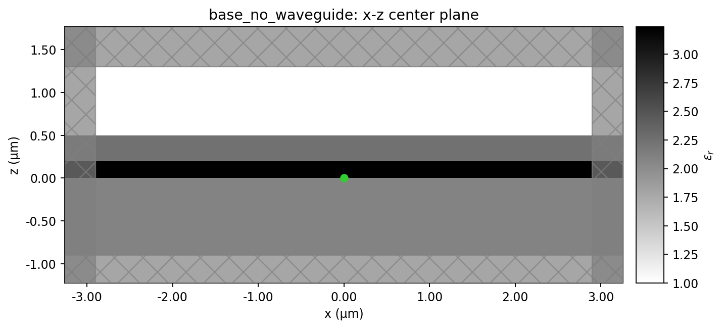
base_no_waveguide xz
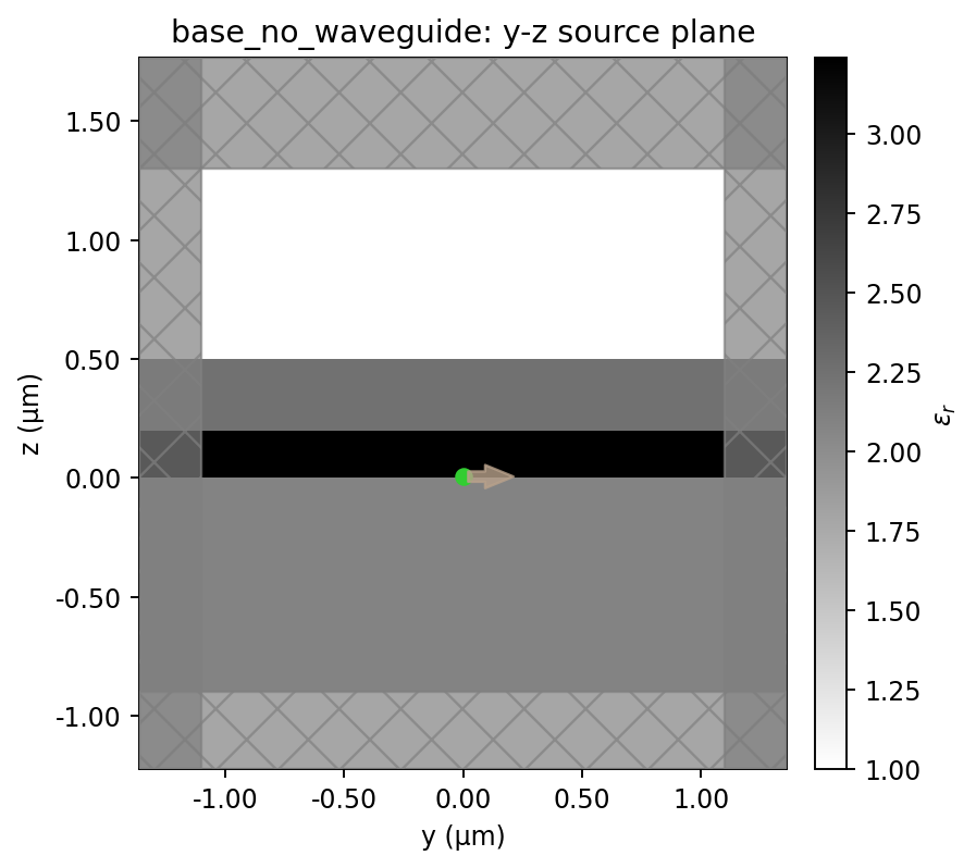
base_no_waveguide yz
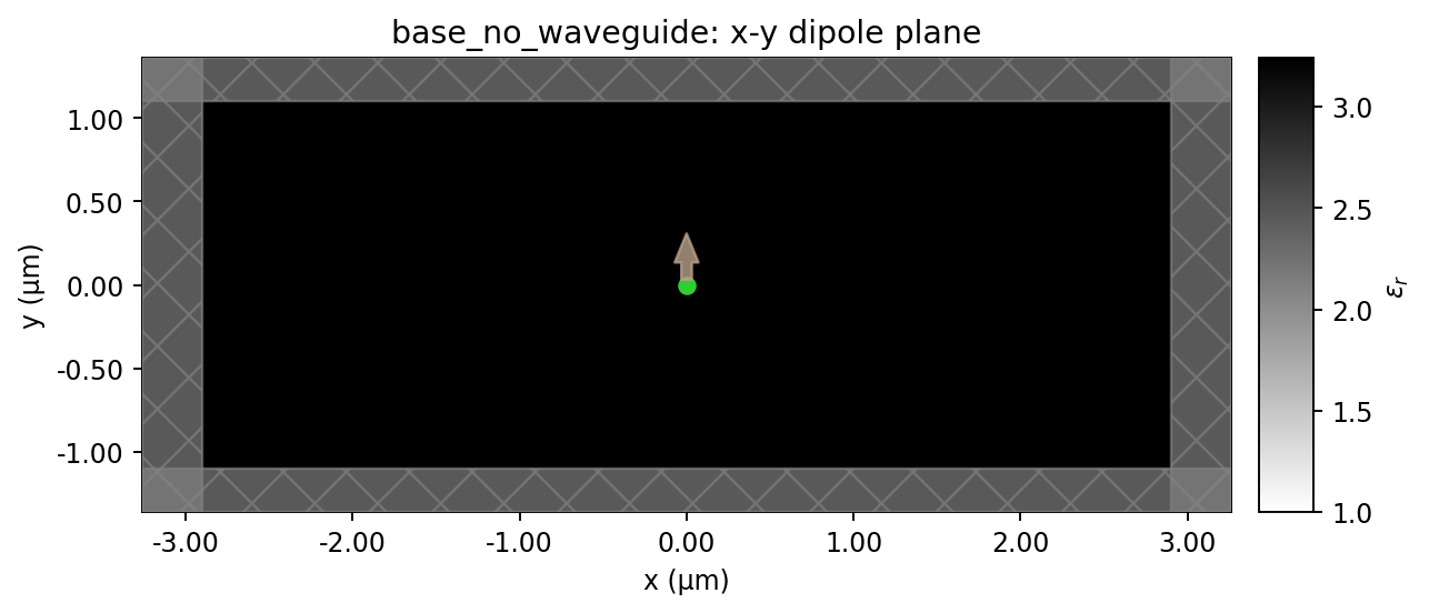
base_no_waveguide xy_dipole
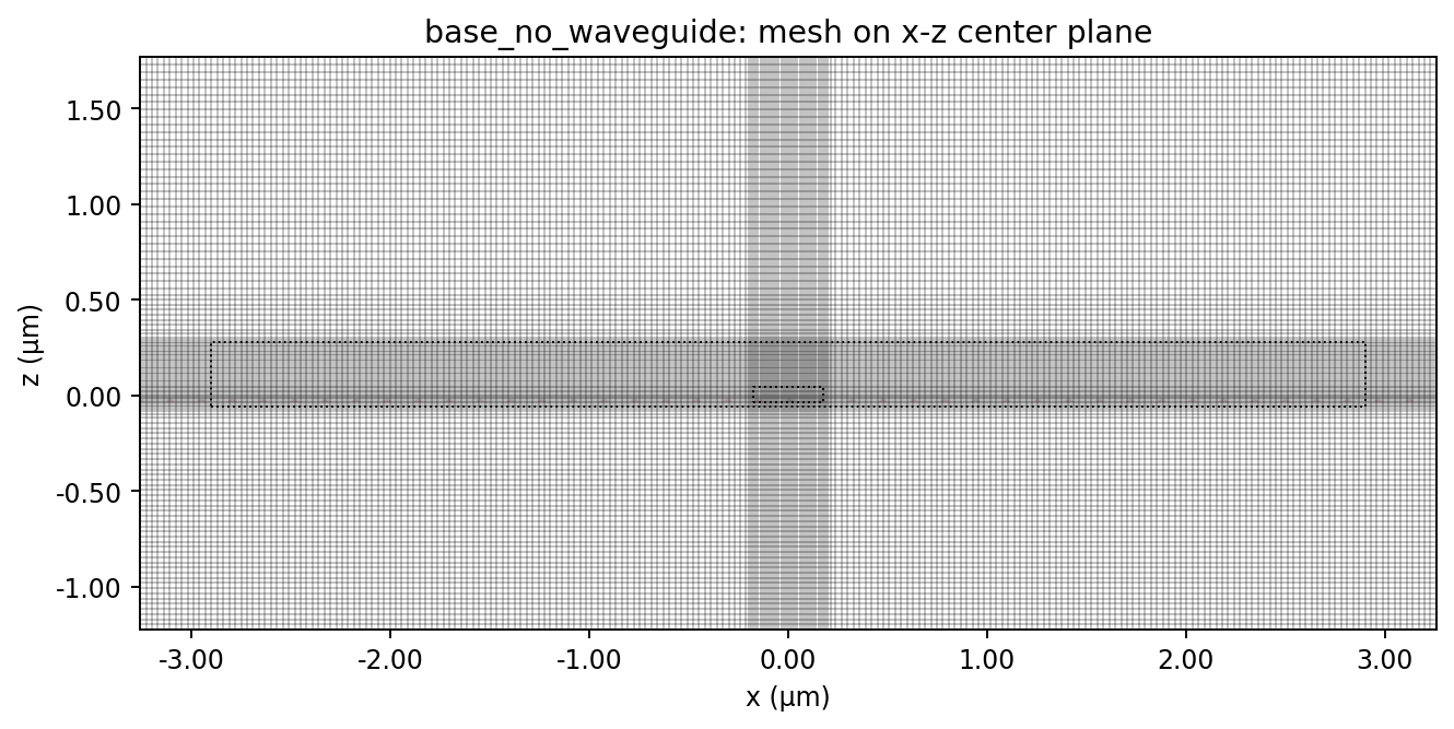
base_no_waveguide mesh_xz
h150_slot050_w450
| Item | Description |
|---|---|
| simulation name | h150_slot050_w450 |
| include slot waveguide | True |
| wavelength grid | 730-830 nm, 21 points |
| dipole | Ey, x=0, y=0, z=155.0 nm |
| substrate | SiO2, n=1.444, z < 0 |
| crystal | n=1.8, 200 nm thick, z=150.0-350.0 nm |
| PVA | n=1.5, 300 nm thick |
| mesh override | dx=30 nm, dy=10 nm, dz=10 nm near slot/crystal |
| Si3N4 | n=2.0, height=150 nm |
| slot width | 50 nm |
| total waveguide footprint | 450 nm |
| rail width | 200.0 nm each |
| mode collection | fundamental mode at x=±2.25 um; summed over both directions |
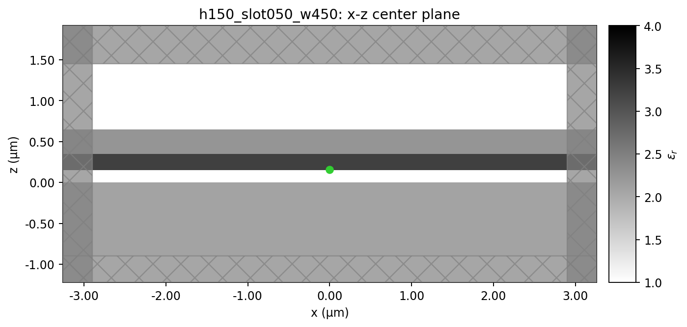
h150_slot050_w450 xz
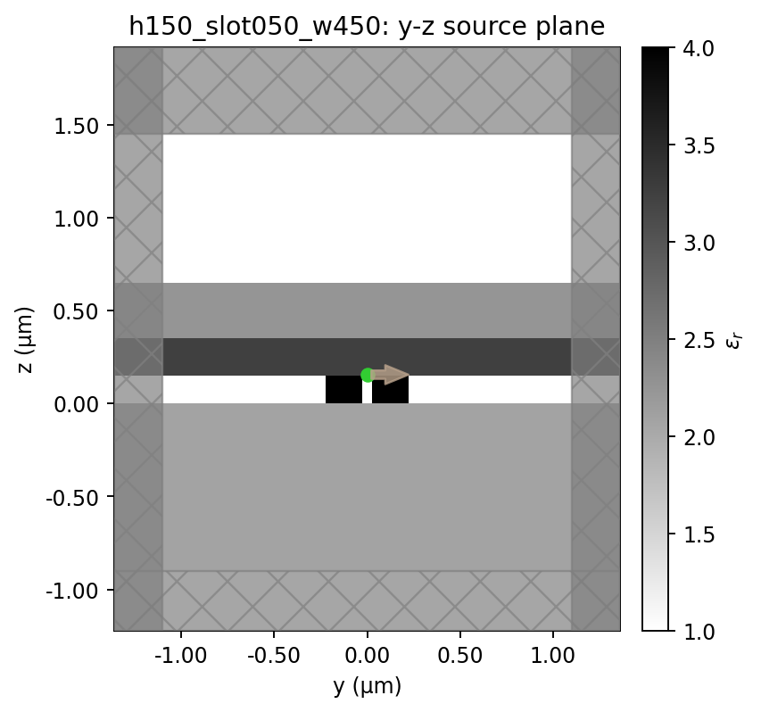
h150_slot050_w450 yz
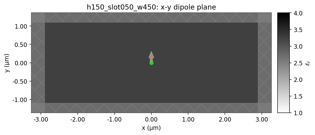
h150_slot050_w450 xy_dipole
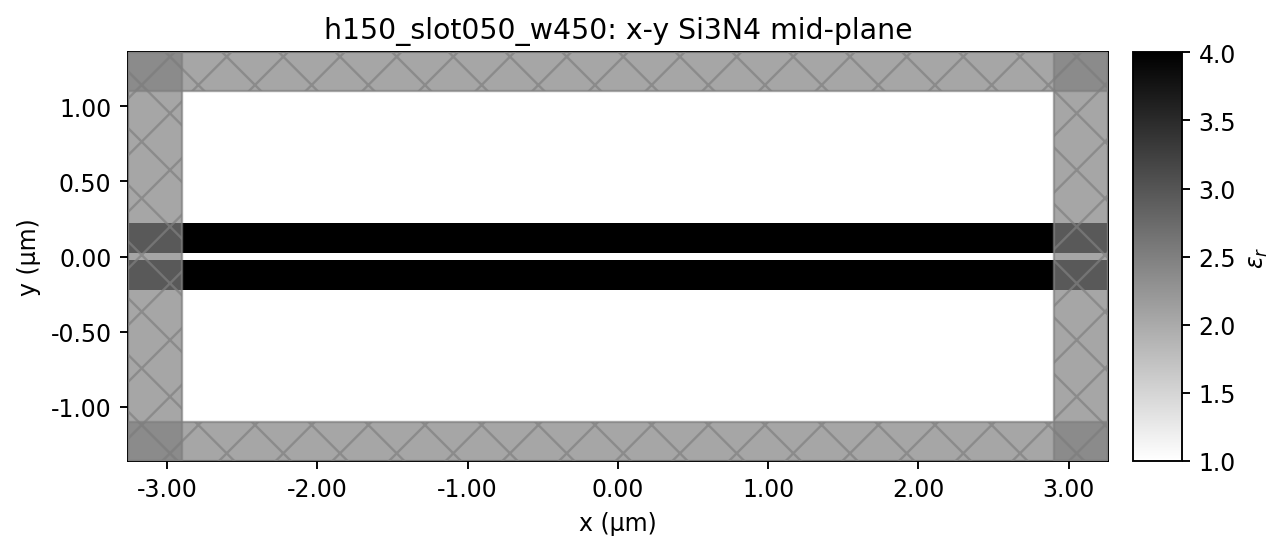
h150_slot050_w450 xy_waveguide
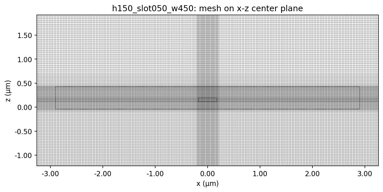
h150_slot050_w450 mesh_xz
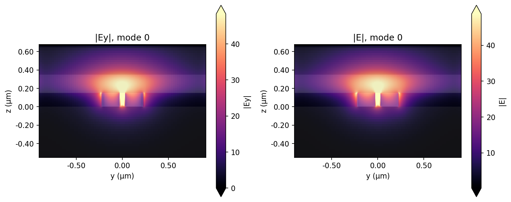
h150_slot050_w450 local mode profile
h150_slot100_w450
| Item | Description |
|---|---|
| simulation name | h150_slot100_w450 |
| include slot waveguide | True |
| wavelength grid | 730-830 nm, 21 points |
| dipole | Ey, x=0, y=0, z=155.0 nm |
| substrate | SiO2, n=1.444, z < 0 |
| crystal | n=1.8, 200 nm thick, z=150.0-350.0 nm |
| PVA | n=1.5, 300 nm thick |
| mesh override | dx=30 nm, dy=10 nm, dz=10 nm near slot/crystal |
| Si3N4 | n=2.0, height=150 nm |
| slot width | 100 nm |
| total waveguide footprint | 450 nm |
| rail width | 175.0 nm each |
| mode collection | fundamental mode at x=±2.25 um; summed over both directions |
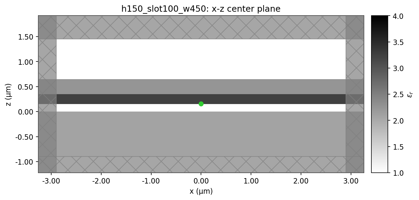
h150_slot100_w450 xz
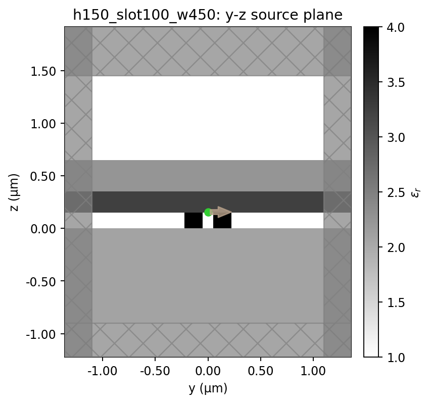
h150_slot100_w450 yz
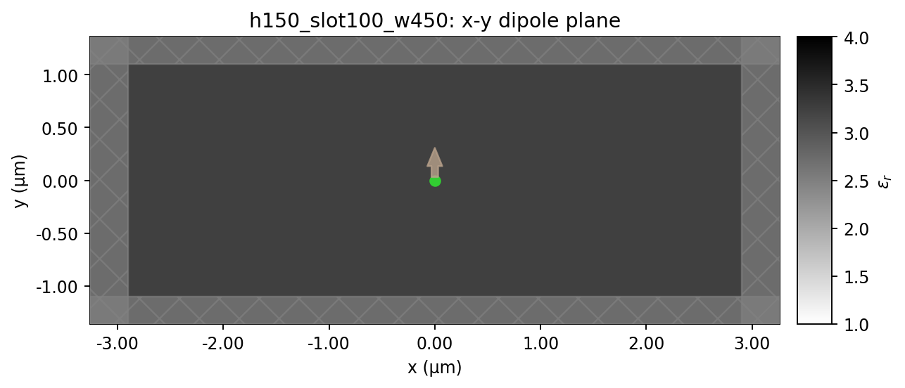
h150_slot100_w450 xy_dipole
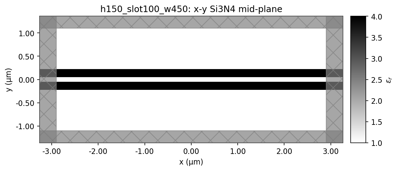
h150_slot100_w450 xy_waveguide
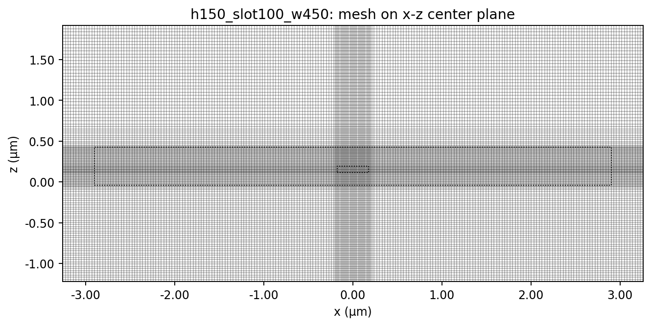
h150_slot100_w450 mesh_xz
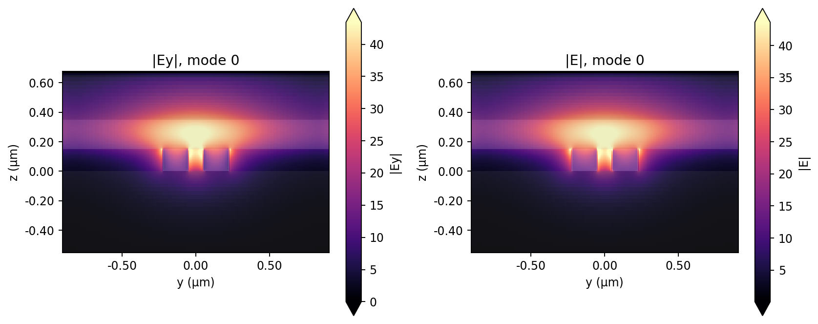
h150_slot100_w450 local mode profile
h150_slot150_w450
| Item | Description |
|---|---|
| simulation name | h150_slot150_w450 |
| include slot waveguide | True |
| wavelength grid | 730-830 nm, 21 points |
| dipole | Ey, x=0, y=0, z=155.0 nm |
| substrate | SiO2, n=1.444, z < 0 |
| crystal | n=1.8, 200 nm thick, z=150.0-350.0 nm |
| PVA | n=1.5, 300 nm thick |
| mesh override | dx=30 nm, dy=10 nm, dz=10 nm near slot/crystal |
| Si3N4 | n=2.0, height=150 nm |
| slot width | 150 nm |
| total waveguide footprint | 450 nm |
| rail width | 150.0 nm each |
| mode collection | fundamental mode at x=±2.25 um; summed over both directions |
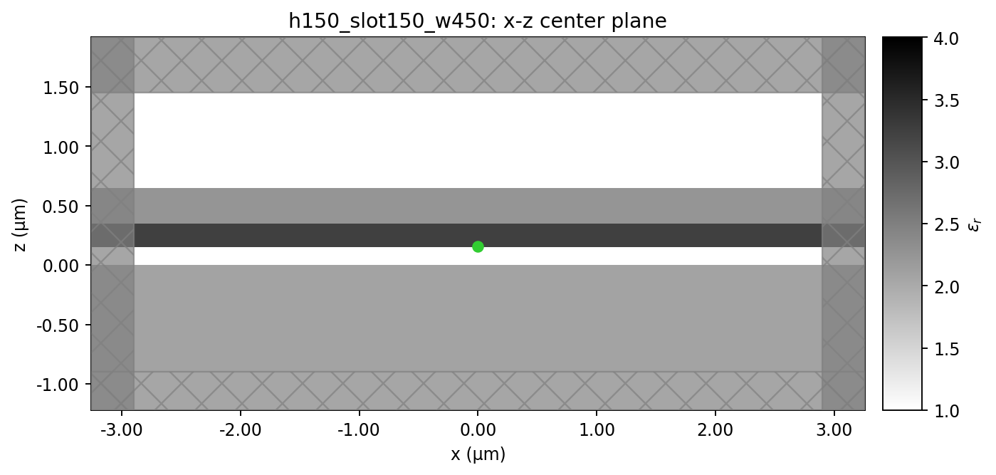
h150_slot150_w450 xz
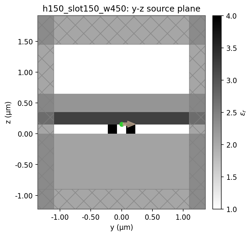
h150_slot150_w450 yz
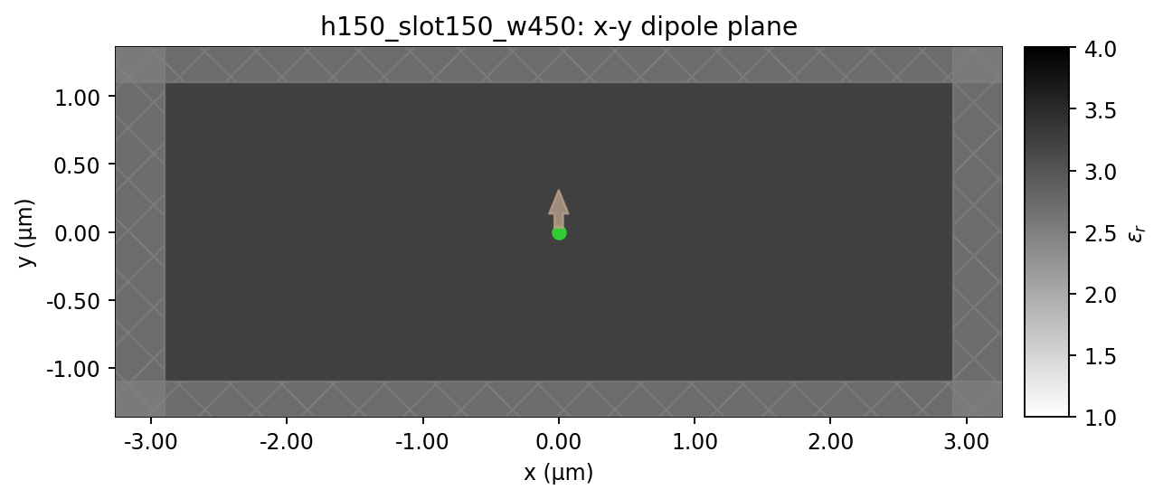
h150_slot150_w450 xy_dipole
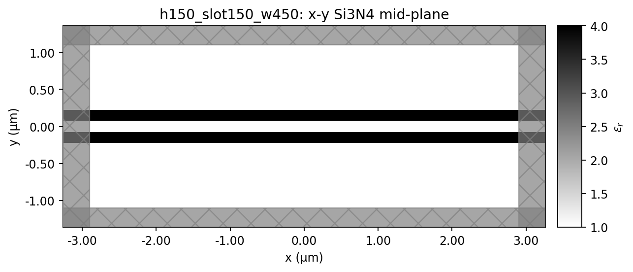
h150_slot150_w450 xy_waveguide
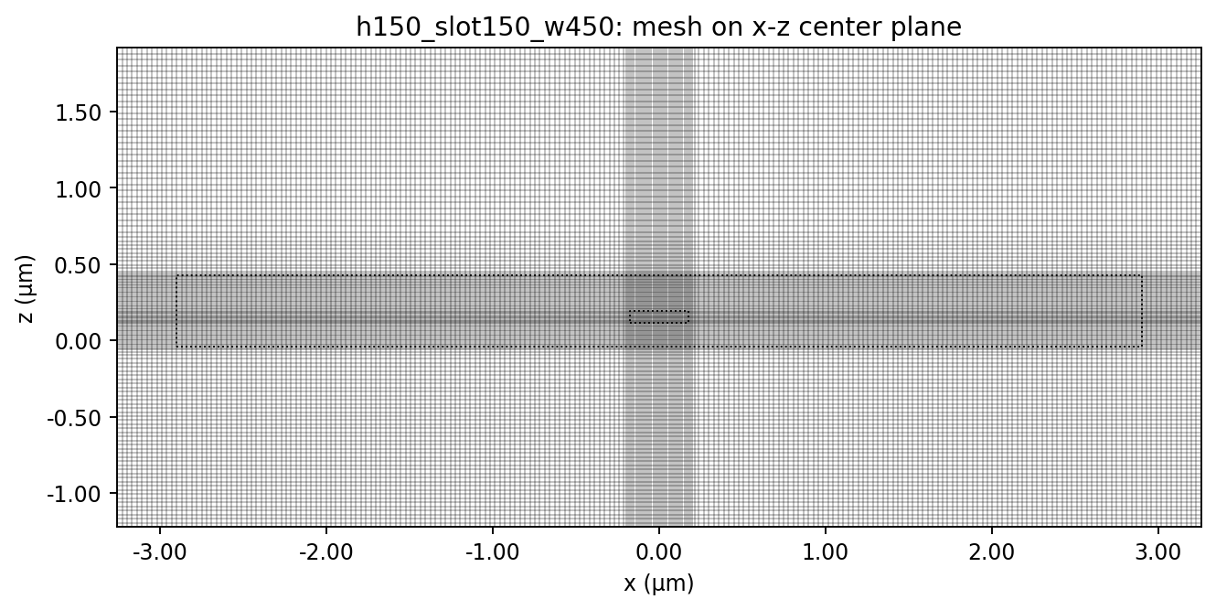
h150_slot150_w450 mesh_xz
h300_slot050_w450
| Item | Description |
|---|---|
| simulation name | h300_slot050_w450 |
| include slot waveguide | True |
| wavelength grid | 730-830 nm, 21 points |
| dipole | Ey, x=0, y=0, z=305.0 nm |
| substrate | SiO2, n=1.444, z < 0 |
| crystal | n=1.8, 200 nm thick, z=300.0-500.0 nm |
| PVA | n=1.5, 300 nm thick |
| mesh override | dx=30 nm, dy=10 nm, dz=10 nm near slot/crystal |
| Si3N4 | n=2.0, height=300 nm |
| slot width | 50 nm |
| total waveguide footprint | 450 nm |
| rail width | 200.0 nm each |
| mode collection | fundamental mode at x=±2.25 um; summed over both directions |
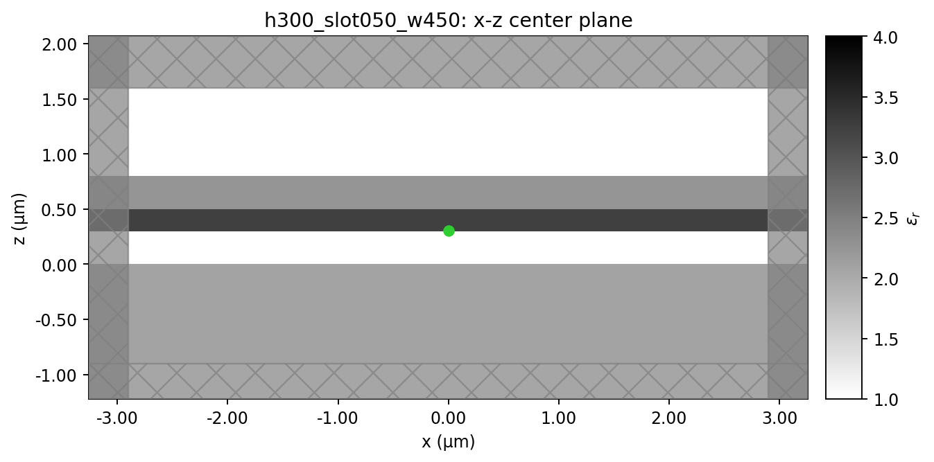
h300_slot050_w450 xz
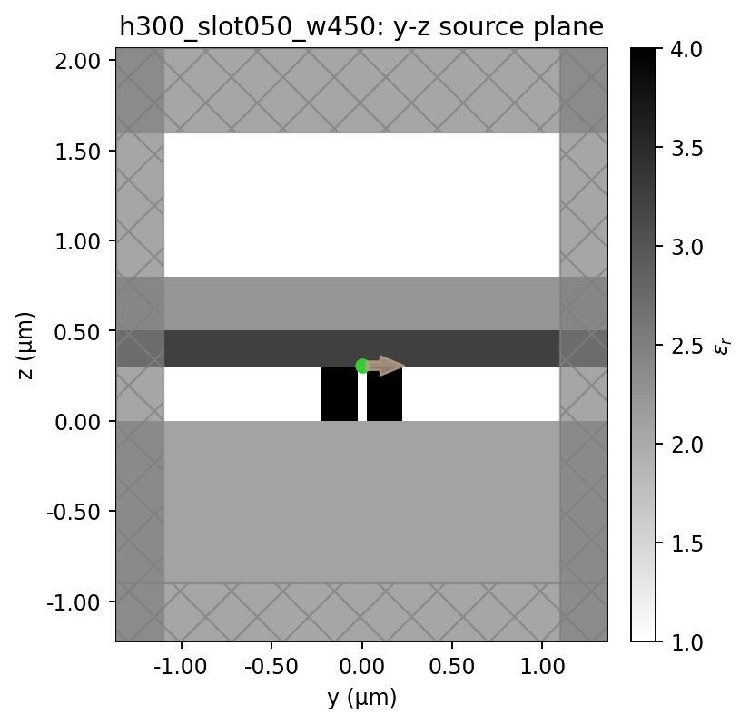
h300_slot050_w450 yz
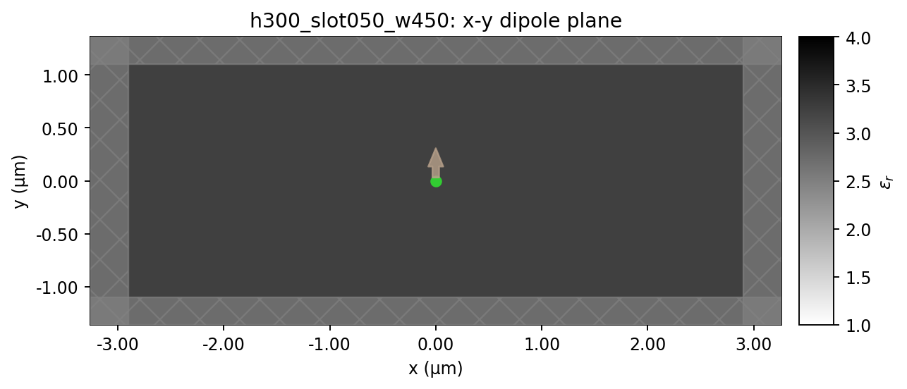
h300_slot050_w450 xy_dipole
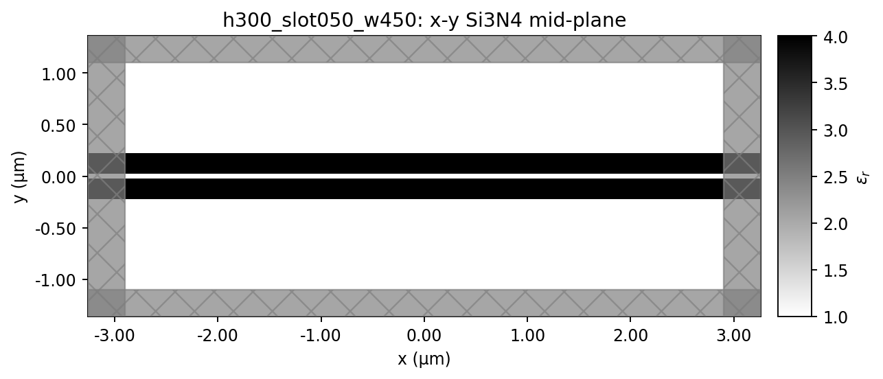
h300_slot050_w450 xy_waveguide
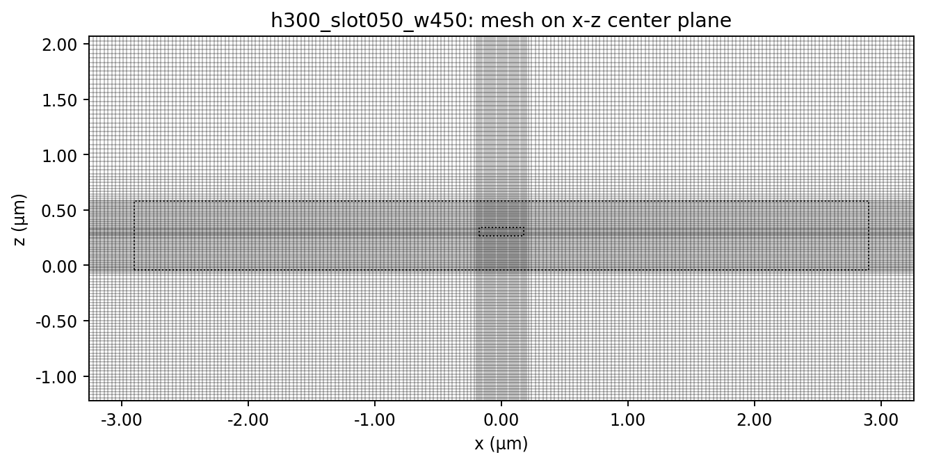
h300_slot050_w450 mesh_xz
h300_slot100_w450
| Item | Description |
|---|---|
| simulation name | h300_slot100_w450 |
| include slot waveguide | True |
| wavelength grid | 730-830 nm, 21 points |
| dipole | Ey, x=0, y=0, z=305.0 nm |
| substrate | SiO2, n=1.444, z < 0 |
| crystal | n=1.8, 200 nm thick, z=300.0-500.0 nm |
| PVA | n=1.5, 300 nm thick |
| mesh override | dx=30 nm, dy=10 nm, dz=10 nm near slot/crystal |
| Si3N4 | n=2.0, height=300 nm |
| slot width | 100 nm |
| total waveguide footprint | 450 nm |
| rail width | 175.0 nm each |
| mode collection | fundamental mode at x=±2.25 um; summed over both directions |
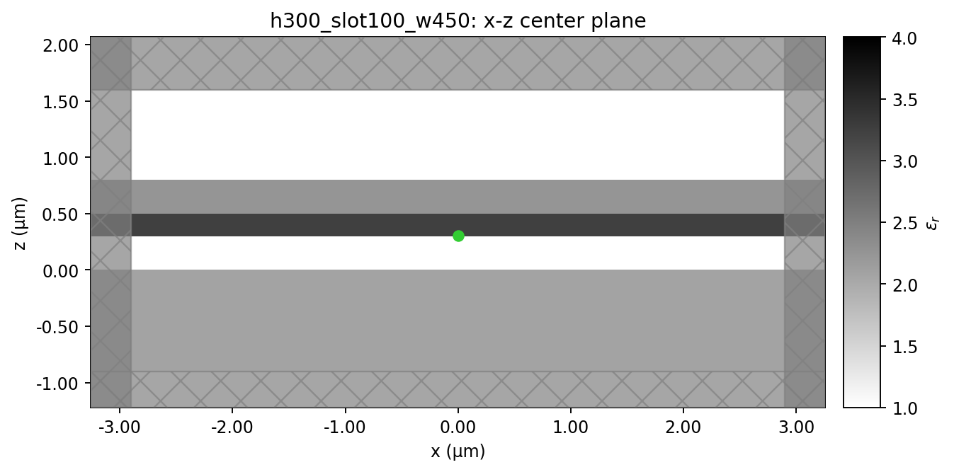
h300_slot100_w450 xz
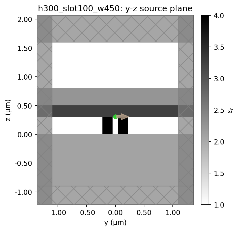
h300_slot100_w450 yz
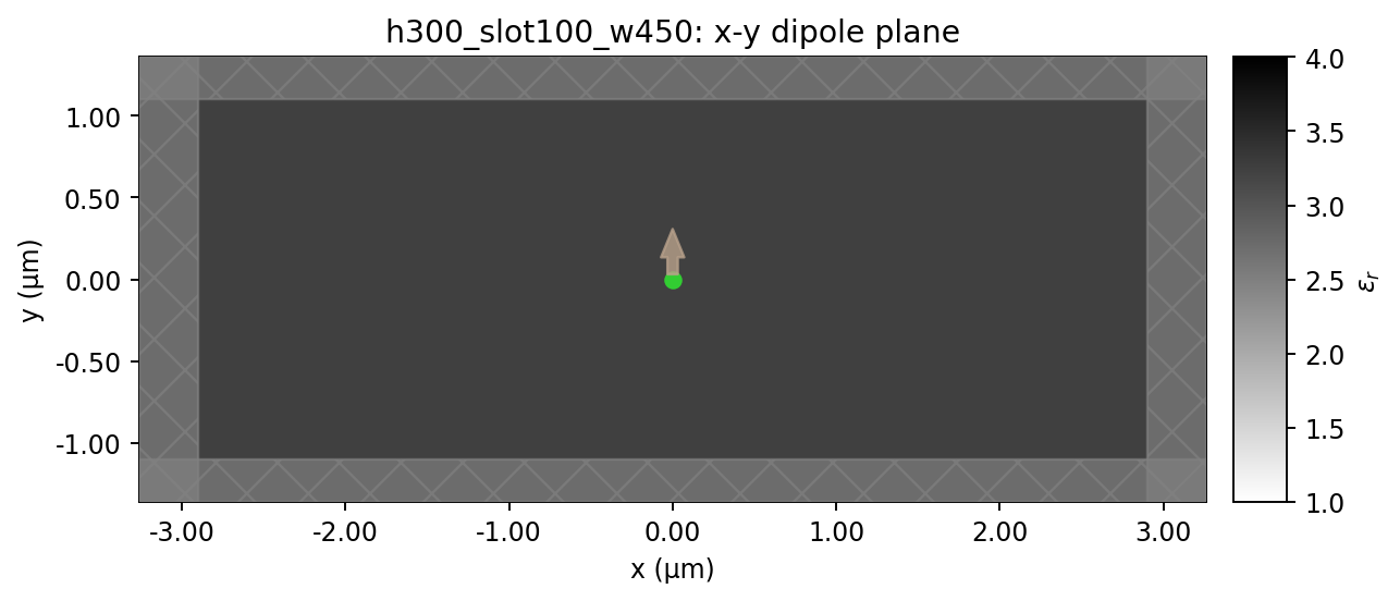
h300_slot100_w450 xy_dipole
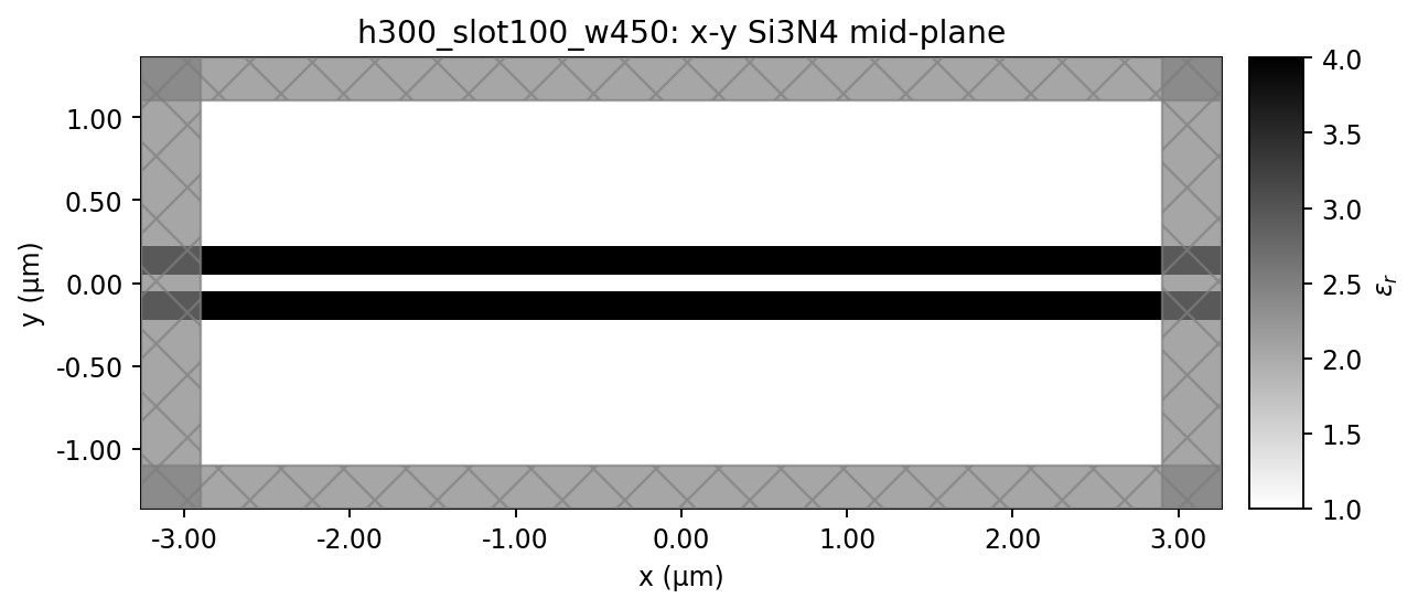
h300_slot100_w450 xy_waveguide
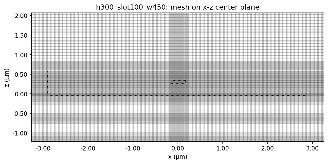
h300_slot100_w450 mesh_xz
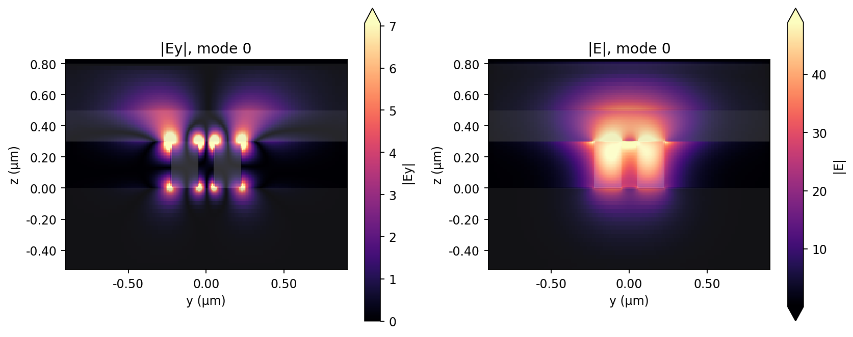
h300_slot100_w450 local mode profile
h300_slot150_w450
| Item | Description |
|---|---|
| simulation name | h300_slot150_w450 |
| include slot waveguide | True |
| wavelength grid | 730-830 nm, 21 points |
| dipole | Ey, x=0, y=0, z=305.0 nm |
| substrate | SiO2, n=1.444, z < 0 |
| crystal | n=1.8, 200 nm thick, z=300.0-500.0 nm |
| PVA | n=1.5, 300 nm thick |
| mesh override | dx=30 nm, dy=10 nm, dz=10 nm near slot/crystal |
| Si3N4 | n=2.0, height=300 nm |
| slot width | 150 nm |
| total waveguide footprint | 450 nm |
| rail width | 150.0 nm each |
| mode collection | fundamental mode at x=±2.25 um; summed over both directions |
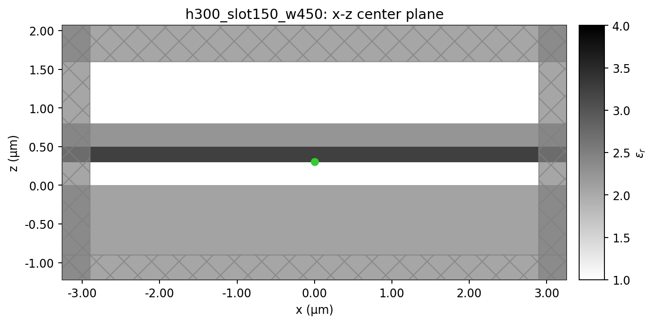
h300_slot150_w450 xz
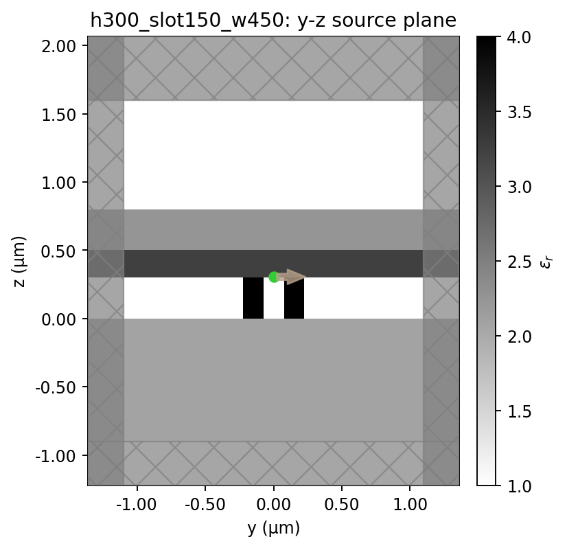
h300_slot150_w450 yz
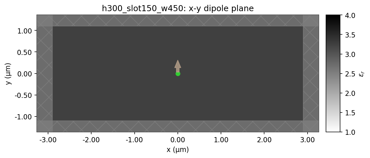
h300_slot150_w450 xy_dipole
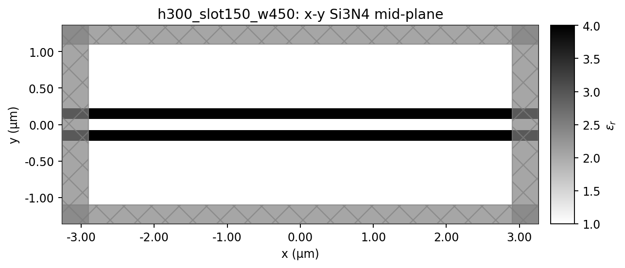
h300_slot150_w450 xy_waveguide
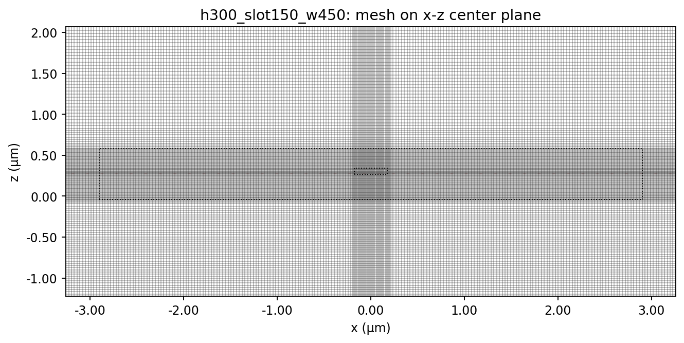
h300_slot150_w450 mesh_xz
Expected post-run outputs
- Spectral total emitted flux for the no-waveguide reference.
- Spectral total emitted flux for every slot-waveguide geometry.
- Spectral guided power into mode 0 at left and right mode monitors.
- Coupling efficiency versus wavelength for each geometry.
- Purcell factor versus wavelength for each geometry.
- 2D heatmaps at 780 nm for Purcell factor and coupling efficiency across height and slot width.
- Field-intensity cross-sections for the best coupling-efficiency geometry.
Final report
Slot Waveguide Purcell FDTD Report
Center-wavelength summary is reported at 780.0 nm.
Summary
| Name | total flux | guided power | coupling efficiency | Purcell | billed cost |
|---|---|---|---|---|---|
| base_no_waveguide | 4419.2 | - | - | 1.0000 | 0.0250 FC |
| h150_slot010_w450 | 10890 | 3315.8 | 0.3045 | 2.4642 | 0.0250 FC |
| h150_slot025_w450 | 10306 | 2676.5 | 0.2597 | 2.3321 | 0.0282 FC |
| h150_slot050_w450 | 8447.5 | 1757.4 | 0.2080 | 1.9115 | 0.0250 FC |
| h150_slot100_w450 | 6364.3 | 994.06 | 0.1562 | 1.4401 | 0.0250 FC |
| h150_slot150_w450 | 5371.7 | 687.78 | 0.1280 | 1.2155 | 0.0250 FC |
| h300_slot010_w450 | 11348 | 3250.7 | 0.2865 | 2.5679 | 0.0253 FC |
| h300_slot025_w450 | 10703 | 2831 | 0.2645 | 2.4219 | 0.0311 FC |
| h300_slot050_w450 | 8717.4 | 1873.1 | 0.2149 | 1.9726 | 0.0250 FC |
| h300_slot100_w450 | 6575.5 | 1007.3 | 0.1532 | 1.4879 | 0.0250 FC |
| h300_slot150_w450 | 5593.7 | 677.39 | 0.1211 | 1.2658 | 0.0250 FC |
Spectral Metrics
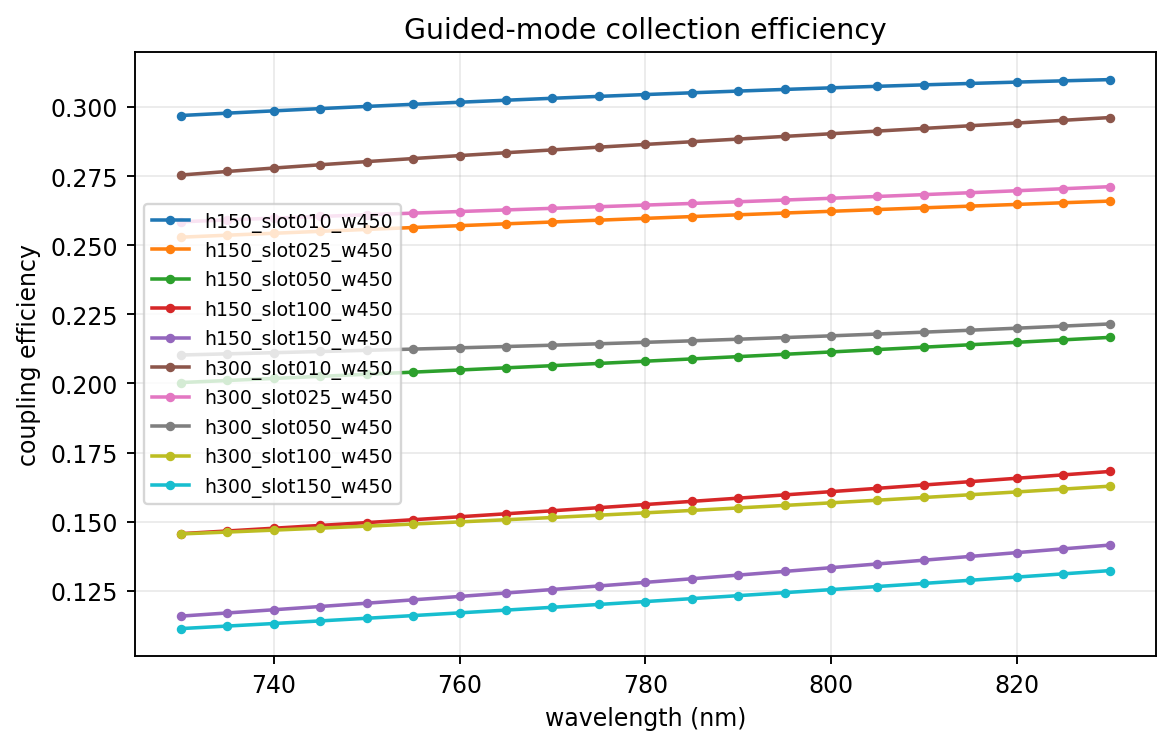
Coupling efficiency versus wavelength
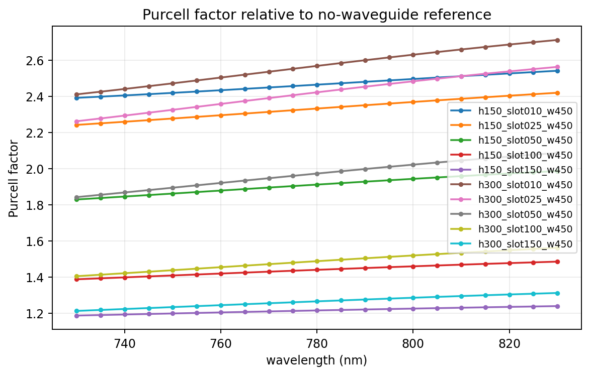
Purcell factor versus wavelength
Sweep Heatmaps
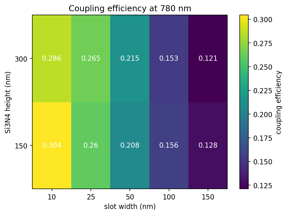
Coupling efficiency heatmap at 780 nm
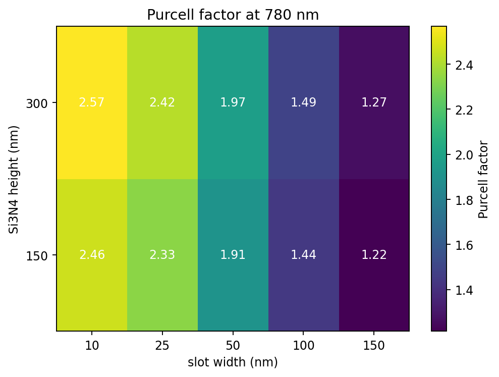
Purcell factor heatmap at 780 nm
Field Intensity Cross-Sections
No-waveguide reference
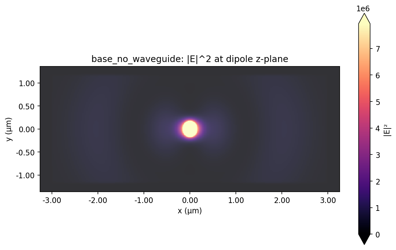
Base reference |E|^2 at dipole plane
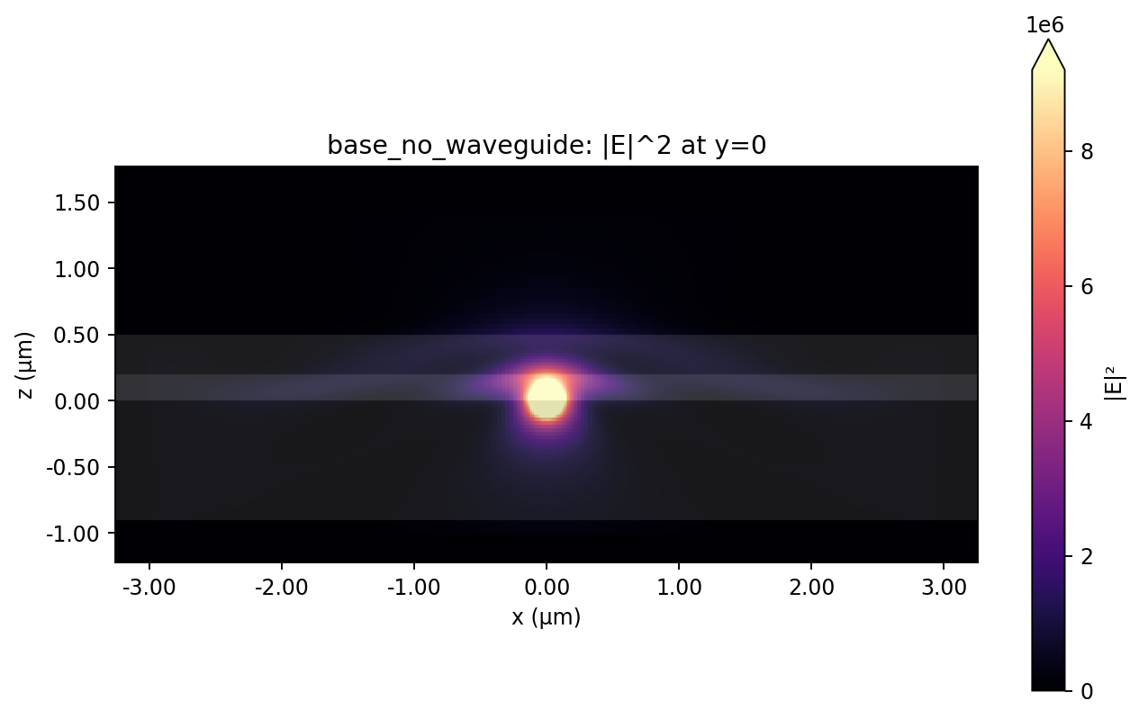
Base reference |E|^2 x-z center plane
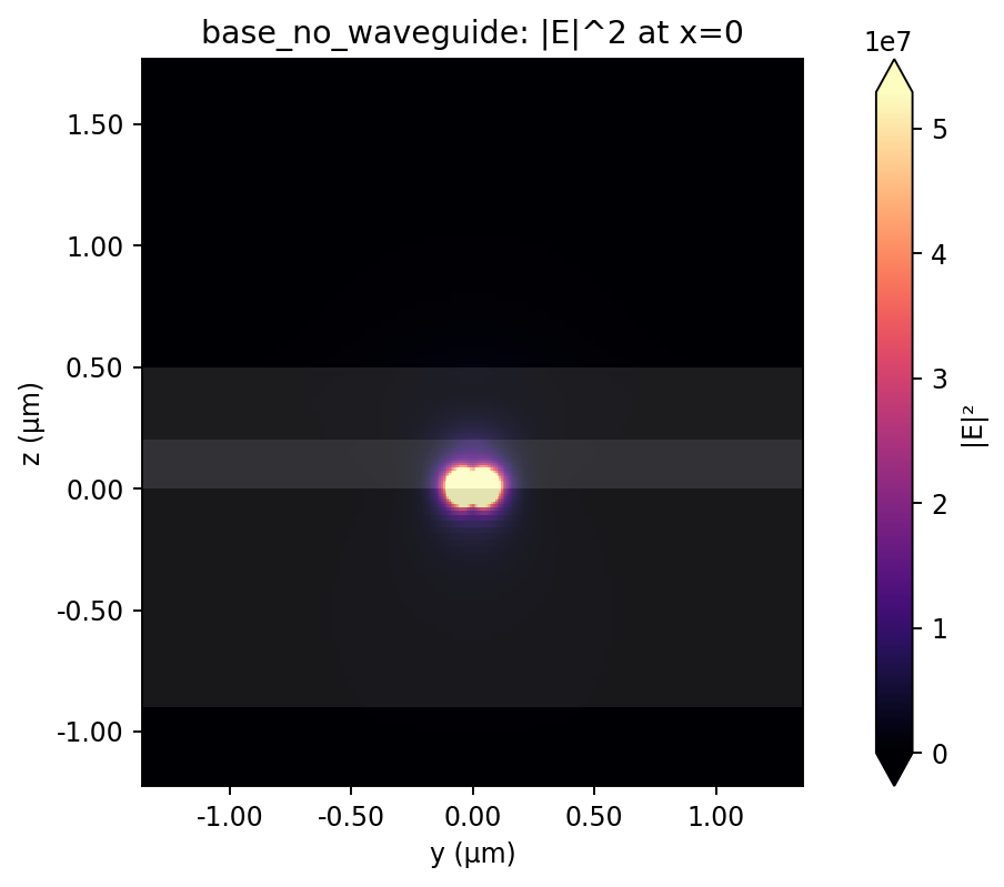
Base reference |E|^2 y-z center plane
Best coupling geometry
Best coupling geometry at 780 nm: h150_slot010_w450.
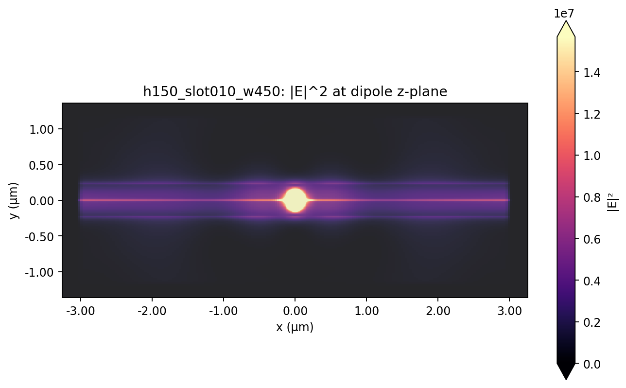
Best-coupling |E|^2 at dipole plane
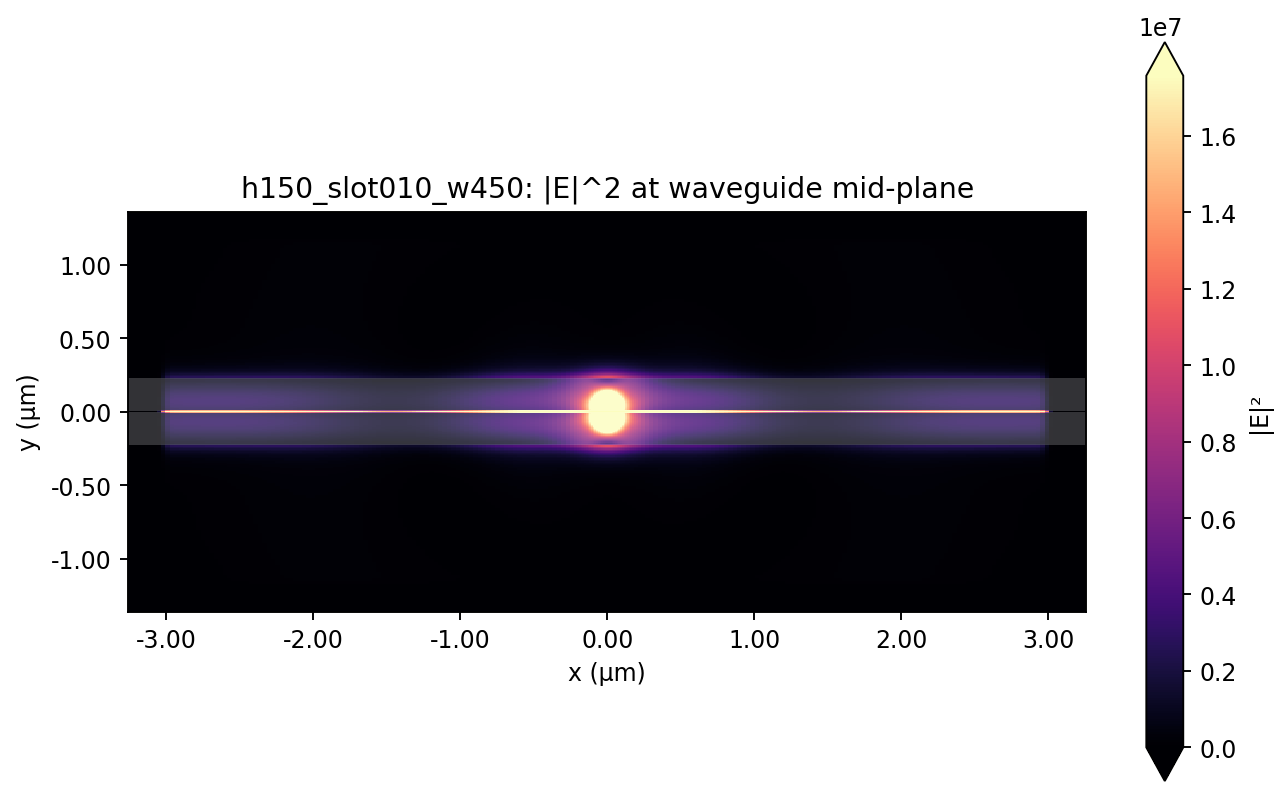
Best-coupling |E|^2 at waveguide plane
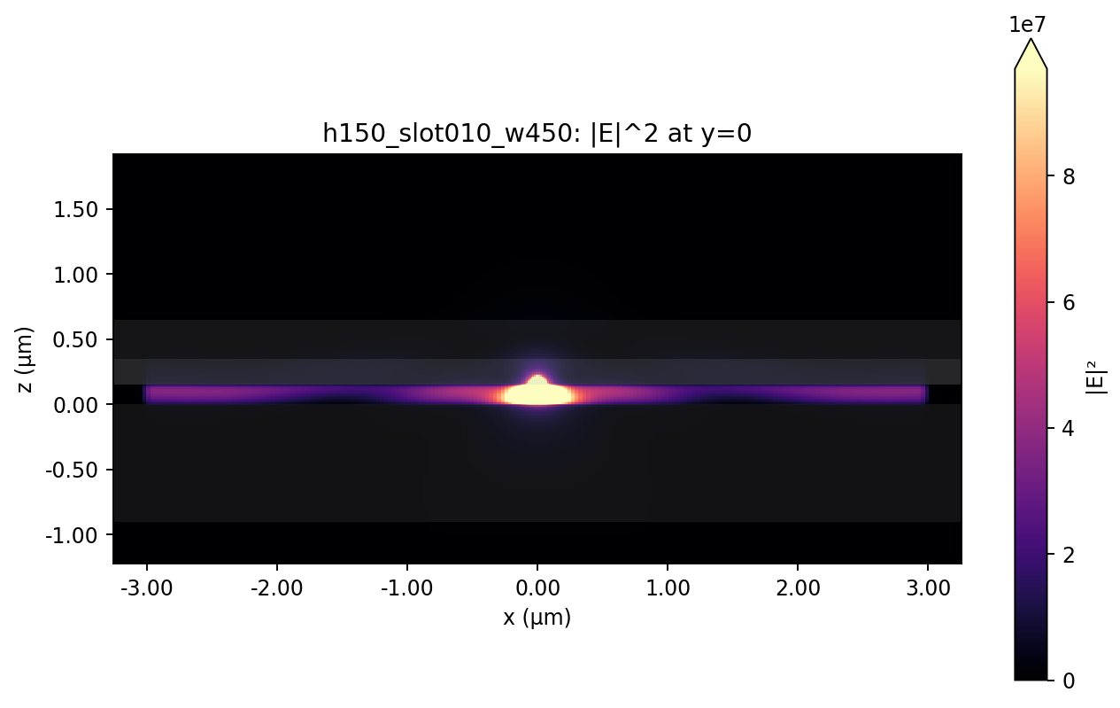
Best-coupling |E|^2 x-z center plane
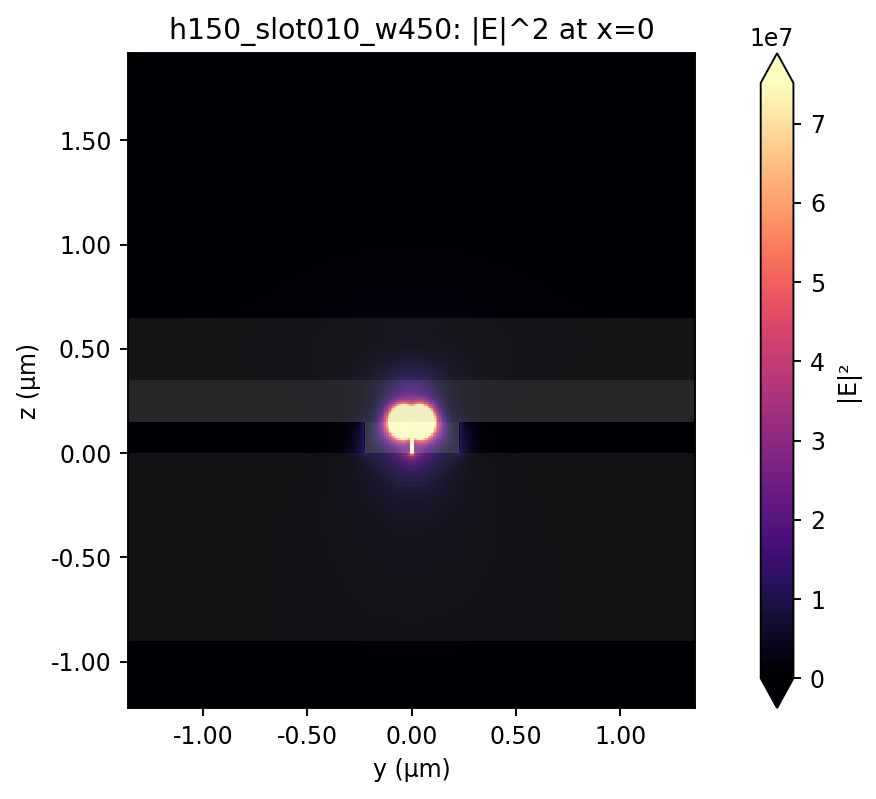
Best-coupling |E|^2 y-z center plane
Notes
- Coupling efficiency sums mode 0 power collected by the left and right mode monitors and divides by the six-surface emitted flux.
- Purcell factor divides each emitted flux spectrum by the no-waveguide reference emitted flux spectrum.
- The raw arrays are saved in
data/metrics.npz.
Downloads
FDTD simulation study only -- no GDS/STL deliverable files exist in this tree.
Source: nanophotonic_devices/cavity_purcell/slot_waveguide_purcell_v1/