Facet-mirror coupling (v3)
Gen 3: crystal stamped on a cleaved facet, fused against a 50nm Ag mirror, NA=0.6 top excitation. Collection 50.5%, excitation 52.0%, cross-talk 2.6%.
FDTD study (tidy3d) of the silver-mirror variant of the v3 device: a
DBT:anthracene crystal stamped on a cleaved Si3N4-waveguide facet, with a
50 nm Ag mirror fused directly behind it, excited from above by an NA=0.6
focused Gaussian beam. See device_architectures/v3/README.md (repo root)
for the full device architecture and the exact geometry spec this study
implements.
Geometry & coordinate convention
x = waveguide-propagation / facet-normal axis, y = in-plane transverse, z =
vertical (z=0 at the waveguide core, z=1.0 um at the device-stack top
surface / air boundary). See config.py's module docstring for the full
structure placement. In short: Si3N4 waveguide (400x300 nm core, SiO2 clad)
terminates at x=0 into a 200 nm anthracene film (n=1.8), fused flush against
a 50 nm Ag mirror at x=0.2-0.25 um. The molecule sits at the center of the
crystal thickness (x=0.1), on-axis with the waveguide (y=0, z=0).
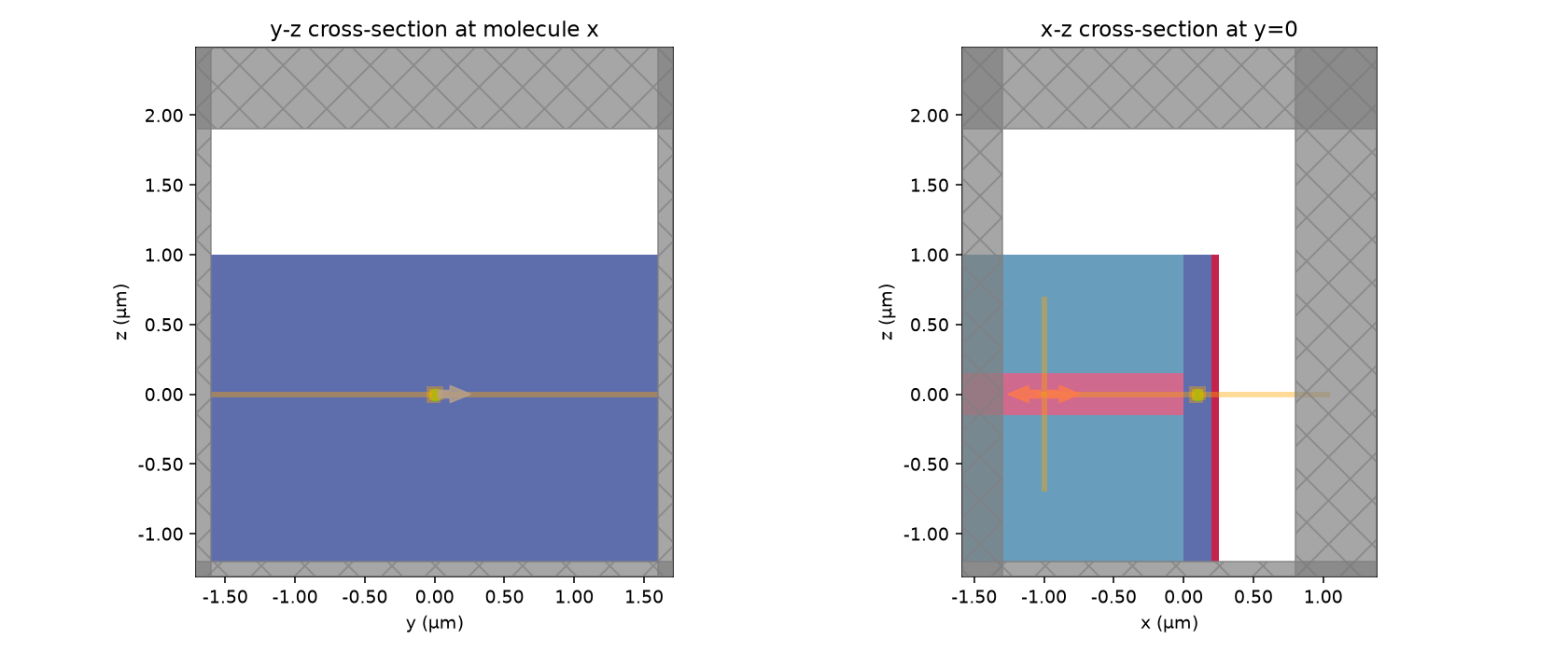
y-z cross-section at the molecule's x location (left) and x-z cross-section at y=0 (right), generated by run_dry_run.py before any billed run.
Simplifications (all deliberate, all budget/scope-driven, flagged
explicitly): crystal and mirror are modeled as broad slabs in y (±1.6 um)
and capped in z at the device-stack top surface — not the true ~50 um
hexagonal crystal footprint, per the PI's explicit "treat as an infinitely
large thin film" instruction. Single wavelength (780 nm) — no spectral
sweep. In-plane (y-oriented) dipole assumed for the molecule's transition
dipole; the true crystallographic orientation isn't yet specified. Stark
electrodes are omitted from this optical simulation (handled separately in
../../../electronics_electrostatics/v3_stark_tuning/) — assumed far
enough from the near-field region not to perturb these results, not
verified by a joint sim.
Method
Three separate FDTD runs plus one free-space reference, all at 780 nm:
- Collection efficiency (
collection.hdf5): a point dipole (y-polarized) at the molecule site. AModeMonitoron the Si3N4 waveguide (1 um back from the facet, away from near-field) measures power in the guided mode propagating away from the facet. Normalized by a smallFluxMonitorbox tightly enclosing the dipole (no lossy material inside the box, so by Poynting's theorem this flux exactly equals the dipole's total radiated power in this environment, regardless of box size). - Excitation efficiency (
excitation.hdf5vs.excitation_reference.hdf5): an NA=0.6GaussianBeamsource (paraxial waist estimatew0 = lambda/(pi*NA)) launched from air, focused at the molecule site.excitation_efficiency = |E(molecule)|^2_with-structure / |E(molecule)|^2_free-space-focus— i.e. how much of the ideal diffraction-limited free-space focus intensity actually reaches the molecule once the real crystal/mirror/ waveguide stack is in the way. The free-space reference is the same source in an entirely homogeneous air domain (no structures) — matching the real sims' air launch medium, not the crystal index, so both sims inject the same nominal source power (an earlier version of this script used a crystal-index reference domain, which is wrong for this reason — see git history — and was corrected before the results below). - Cross-talk (
crosstalk.hdf5): the same excitation beam, same structure, no dipole present. Measures power leaking directly into the same waveguide mode monitor, normalized by the launched beam power (aFluxMonitorspanning the domain in air, just below the source, before the beam hits any structure).
Results (780 nm, this geometry)
| Metric | Value |
|---|---|
| Collection efficiency (dipole -> guided mode) | 50.5% |
| Excitation efficiency (vs. ideal free-space NA=0.6 focus) | 52.0% |
| Cross-talk (excitation beam -> waveguide, no molecule) | 2.6% |
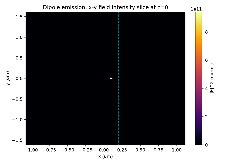
Dipole emission (collection study): |E|^2 in the x-y plane at z=0. Bright spot at the dipole (x=0.1); the guided-mode intensity is visible propagating in -x toward the mode monitor.
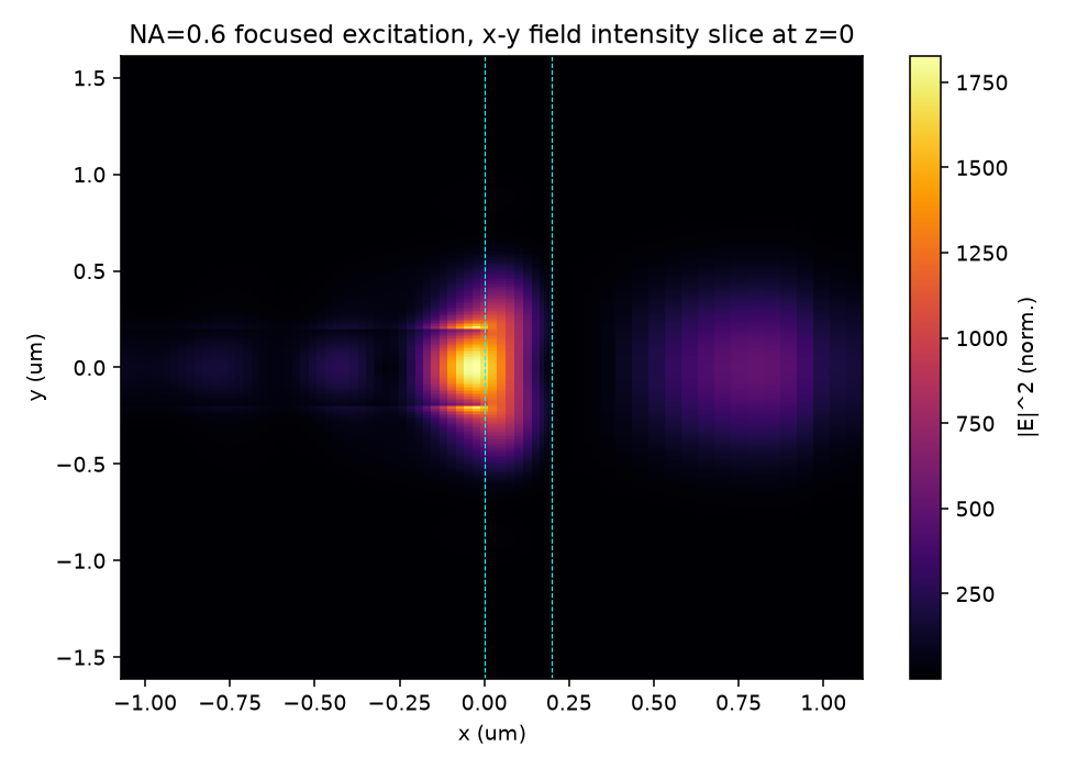
NA=0.6 excitation focus (excitation study): the tight focus at the molecule site (x=0.1) plus a mirror-reflected secondary lobe further into the structure — the loss mechanism behind the 52.0% excitation efficiency, see Interpretation below.
Raw numbers in data/results.json. Regenerate everything with:
.venv/bin/python run_dry_run.py   # free cost-estimate + geometry sanity plot
.venv/bin/python run_study.py     # billed FDTD run (~0.13 FlexCredits total)
.venv/bin/python reporting.py     # analysis + field figures
Total billed cost for this study: ~0.13 FlexCredits (well under the 2-FlexCredit budget for this study — early shutoff triggered fast on every run since the geometry is small and lossless except at the Ag mirror).
Interpretation & caveats
- 50.5% collection is high relative to other in-plane coupling studies in
this repo (e.g.
anthracene_inplane_cavity_v1reports ~14% for a related but different geometry). This is expected and not a red flag: the crystal and mirror here are translationally uniform in y (no finite-crystal edge losses), the dipole sits exactly on-axis with the waveguide core with zero gap to the facet, and a mirror immediately behind the emitter is a favorable coupling geometry (constructive image-dipole interference toward the guide). Treat this as an idealized best-case estimate for this exact alignment, not a fabrication-tolerant number — a real, finite, possibly-misaligned 50 um crystal stamp will do worse. - The 52% excitation efficiency reflects real physical loss mechanisms
(Fresnel reflection at the air/crystal interface, index-mismatch
aberration of the focus, and mode conversion into the mirror/waveguide
near-field) rather than any numerical artifact — the field figure
(
figures/excitation_field_slice.png) shows a mirror-reflected secondary lobe forward of the crystal, consistent with genuine loss to a reflected beam that doesn't return to the focus. - Cross-talk (2.6%) is the fraction of excitation light directly reaching the collection channel with no molecule present — this sets a floor on achievable signal-to-background for single-molecule detection through this waveguide and should be compared against the actual single-molecule photon rate once collection efficiency x count rate is known.
How much to trust the 2.6% cross-talk number
Checked this directly (verify_crosstalk.py, data/crosstalk_verification.json)
after being asked whether it might be a numerical artifact:
| Check | Cross-talk |
|---|---|
| Baseline (16 steps/wavelength, 780 nm) | 2.63% |
| Finer mesh (18 steps/wavelength, 780 nm) | 2.65% |
| Detuned -10 nm (770 nm) | 2.68% |
| Detuned +10 nm (790 nm) | 2.58% |
All four land within a 2.58-2.68% band — not sitting on a sharp interference fringe and not a mesh-resolution artifact; the number is numerically stable.
That said, stable-in-this-model is not the same as an accurate real-device prediction. This simulation only captures one cross-talk mechanism: direct diffractive/scattering leakage of the focused pump beam into the guided mode, in an idealized, defect-free, translationally-broad (not the true finite ~50 um) crystal/mirror geometry. It excludes essentially everything that dominates cross-talk in real hardware: surface roughness scattering, the true finite crystal edge, fiber/lens misalignment, stray reflections in the packaging, and any detector-side leakage. Treat 2.6% as a lower-bound estimate of this one mechanism, not a real-device cross-talk prediction — real hardware should be expected to do worse, not better.
Downloads
FDTD simulation study only -- no GDS/STL deliverable files exist in this tree (chip-scale GDS lives in v3_splitter_and_lens).
Source: nanophotonic_devices/emitter_coupling/anthracene_facet_mirror_coupling_v3/