V3 Stark-tuning electrostatics
2D FEM for the Gen 3 silver-mirror molecule site: E-field per volt from the in-plane Stark-tuning electrodes.
2D finite-element (scikit-fem) electrostatics for the device-v3
silver-mirror molecule site: how much E-field does a given Stark-electrode
drive voltage produce at the molecule, and what's the field distribution
across the cross section. Source geometry: device_architectures/v3/README.md
(repo root), "Molecule-site geometry" section.
TL;DR result
dEy/dV = -2.08 x 10⁴ V/m per volt of electrode
drive amplitude (electrodes at -V/+V differential, mirror grounded, 2 um
gap). Over the ±20 V sweep range that's ±0.42 MV/m (±4.2 kV/cm)
of in-plane field at the molecule. See figures/field_vs_voltage.png and
Results below. This is a plain E-field-per-volt number, not a
frequency shift -- see Converting to a Stark shift.
Method
scikit-fem finite elements, same tool as
../v1_electrostatics_capacitor/electrostatics_capacitor_scikit_fem.ipynb,
adapted to this cross section. This is a source-free Laplace solve
(piecewise-constant permittivity per region, no volume charge) with
Dirichlet boundary conditions on the electrodes, mirror, and a padded
"far-field ground" outer boundary -- same house convention as
../conductor_island_efield_study/.
Electrodes and the mirror are modeled as Dirichlet-pinned regions over
their entire footprint (not just their boundary), so no metal
permittivity is needed -- same trick the v1 notebook uses.
Geometry and coordinate system
Why this cross section: the task is Stark tuning by the in-plane electrodes + mirror, and that arrangement is transverse to the waveguide, not along it. So we solve the (y, z) plane transverse to the waveguide propagation direction, cut at the molecule's x location inside the 200 nm DBT:anthracene crystal film. Origin (y, z) = (0, 0) is the Si3N4 waveguide center, matching the v3 README.
- y: in-plane, perpendicular to the waveguide
- z: vertical (wafer-normal) height
Layer stack (z, bottom to top) -- see solver.py module docstring for
the exact numeric levels:
| z region | material | source / assumption |
|---|---|---|
| z < -2.0 um (outer boundary) | grounded far-field / Si handle wafer | ASSUMPTION: the Si substrate is treated as grounded and far enough away not to matter; not stated in the v3 README |
| -2.0 .. -0.15 um | SiO2 lower cladding | eps_r = 3.9 |
| -0.15 .. +0.15 um | Si3N4 waveguide core, | y |
| +0.15 .. +0.8 um | SiO2 mid cladding ( | y |
| +0.8 .. +1.0 um | DBT:anthracene crystal, full width | 200 nm thickness from v3 README |
| z = +1.0 um | Ag mirror (Dirichlet boundary, bonded to crystal top) | 50 nm mirror from v3 README, modeled as a boundary condition (ideal conductor, E=0 inside) rather than a meshed metal volume |
Molecule site: y = 0, z = 0.9 um (center of the crystal film thickness, directly above the waveguide/gap center) -- the natural, maximally symmetric choice given the v3 README doesn't specify the exact in-crystal molecule position.
One explicit interpretation call
The v3 README's molecule-site geometry list gives "z > 1 um: air" / "z < 1 um: 50 nm Ag mirror" and, separately, "Si3N4 waveguide centered at (y,z) = (0,0)" and "1 um SiO2 cladding above [the waveguide]". Read completely literally these are hard to reconcile (a metal mirror can't occupy all of z < 1 um if the waveguide also sits at z = 0). We interpreted this as: the mirror sits ~1 um above the waveguide, with the crystal (in the silver-mirror variant) bonded directly to its underside, and "1 um SiO2 cladding above" describes the total dielectric stand-off from the waveguide up to that mirror/crystal interface. This is the most physically sensible reading we found and produces a normal molecule-in-a-cavity picture, but it is an interpretation, not a literal transcription -- flagged for the PI to confirm.
Stark electrodes: modeled as vertical metal "sidewalls" flanking the
waveguide in y, spanning the full z-band from the waveguide bottom up to
the crystal bottom (z in [-0.15, 0.8] um) -- i.e. in-plane electrodes that
also extend up close to the crystal, per the v3 README's "in-plane...
flanking the waveguide" description. Electrode inner edge sits
ELECTRODE_GAP = 2.0 um outward from the waveguide edge (so at y =
±2.3 um), electrode width 3.0 um outward from there.
- Electrode gap = 2 um is an ASSUMPTION, chosen in the 1-3 um range suggested by the task: close enough to get a usable field at the molecule, far enough that the metal shouldn't clip the guided optical mode (standard rule of thumb for photonic tuning electrodes; not a quantitative mode-overlap calculation).
- Reference choice: mirror grounded (0 V), electrodes driven differentially at -V / +V. Differential drive keeps the molecule near 0 V DC and (for this symmetric geometry) roughly doubles the E-field per volt of drive amplitude vs. single-ended drive.
Materials (relative permittivity, DC/low-frequency -- NOT optical index)
| Material | eps_r used | Status |
|---|---|---|
| SiO2 | 3.9 | Standard literature value; matches EPS_R_SIO2 already used in ../conductor_island_efield_study/run_study.py |
| Si3N4 (LPCVD) | 7.5 | Literature range for LPCVD Si3N4 DC permittivity is ~7-9 (distinct from its optical index n~2.0, which is the wrong quantity for a DC problem). The waveguide is a small feature far from the molecule here, so this has little effect on the headline result. |
| DBT:anthracene | 3.2 | PLACEHOLDER, not a literature-measured DC value. We searched but could not find a specific, reliable citation for anthracene's static dielectric constant. Anthracene is a nonpolar molecular crystal (D2h symmetry, no permanent dipole), so its low-frequency dielectric response should be dominated by the same electronic polarizability that sets the optical index (n=1.8, per the v3 README), with only a modest extra contribution -- physically we'd expect eps_r,DC only somewhat above n^2 = 3.24. We used eps_r = 3.2 as an order-of-magnitude estimate. Flagged for the PI: replace with a real literature value if the precise slope matters; the crystal is thin (200 nm) and sandwiched between two nearly-equipotential surfaces (electrodes below, mirror above) so we'd guess this parameter's effect on the molecule field is second order, but that has not been separately checked. |
| Ag mirror, electrodes | n/a (ideal conductor) | Dirichlet boundary / Dirichlet-pinned region, not meshed as a dielectric |
Numerics
- Tensor-product triangular mesh (
skfem.MeshTri.init_tensor), refined to 20 nm spacing in the gap/crystal/waveguide-edge region and near every electrode edge (field varies fastest there), 100 nm in transition zones, 500 nm in the far field. Baseline mesh: ~24k DOFs / ~47k elements. - Mesh convergence check (not a full convergence study -- this is a report-quality estimate, not a metrology-grade one): re-solved the V=±1V case on a ~4x-denser mesh (~91k DOFs). Ey at the molecule: -20833 V/m (baseline) vs. -20666 V/m (fine mesh), a 0.8% difference. Good enough for the linear slope reported here.
- Solve is linear in the applied voltages (pure Laplace, no space
charge), confirmed numerically: the 21-point sweep is exactly linear
(see
data/sweep_results.npz,np.polyfitresidual is essentially zero).
Results
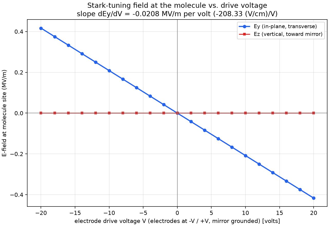
The core result: Ey and Ez at the molecule vs. electrode drive voltage V (electrodes at -V/+V, mirror grounded), V in [-20, +20] V.
- dEy/dV = -2.083 x 10⁴ V/m per volt (in-plane component, driven by the electrodes -- this is the dominant term)
- Ez (vertical, toward the mirror) stays essentially zero across the sweep, as expected by the left-right symmetry of the differential-drive geometry at y = 0 (largest observed |Ez| in the sweep is ~12 V/m at V=20, five orders of magnitude below Ey -- consistent with numerical noise/mesh asymmetry, not a real effect)
- At the sweep extremes (±20 V): Ey = -/+ 4.17 x 10⁵ V/m (0.42 MV/m, 4.2 kV/cm)
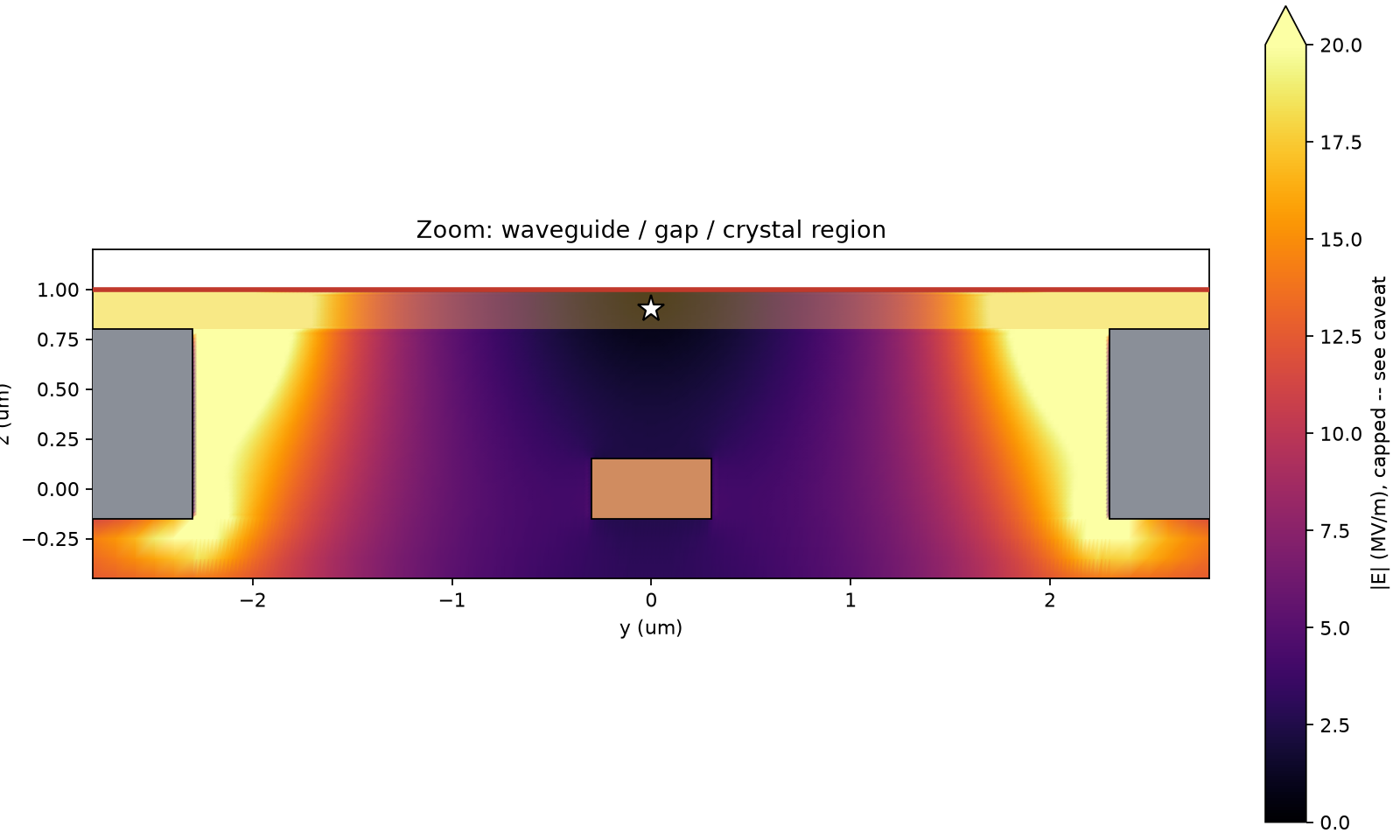
|E| map for the V=-20V/+20V case, zoomed to the waveguide/gap/crystal region, with geometry outlines and the molecule site marked. Color scale is capped at 20 MV/m; the true 99.5th-percentile field in this case is ~118 MV/m, occurring right at the sharp electrode top corners. That's a mesh/geometry artifact (idealized 90-degree conductor corners produce a mathematically divergent field; a real fabricated electrode has a finite corner radius that regularizes this to something well below the FEM value) -- not a claim that the device sees 118 MV/m anywhere. The uncapped map is not shown because it washes out the crystal/gap region, which is what matters for this study.
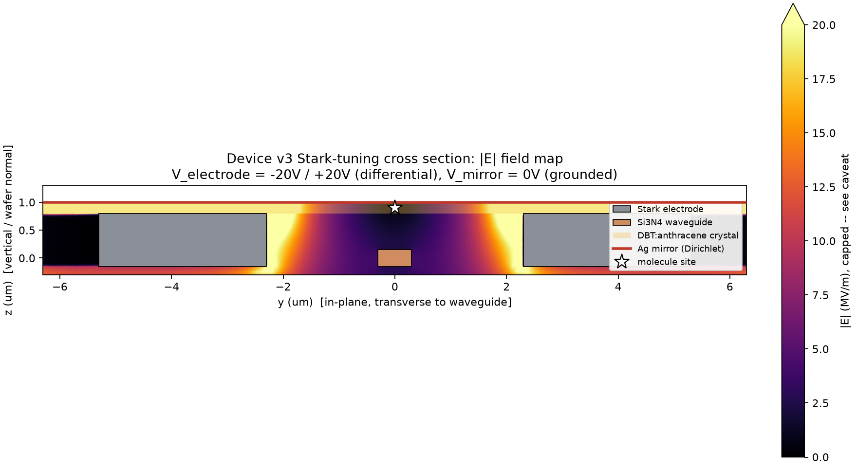
Same case, full simulation domain (unzoomed).
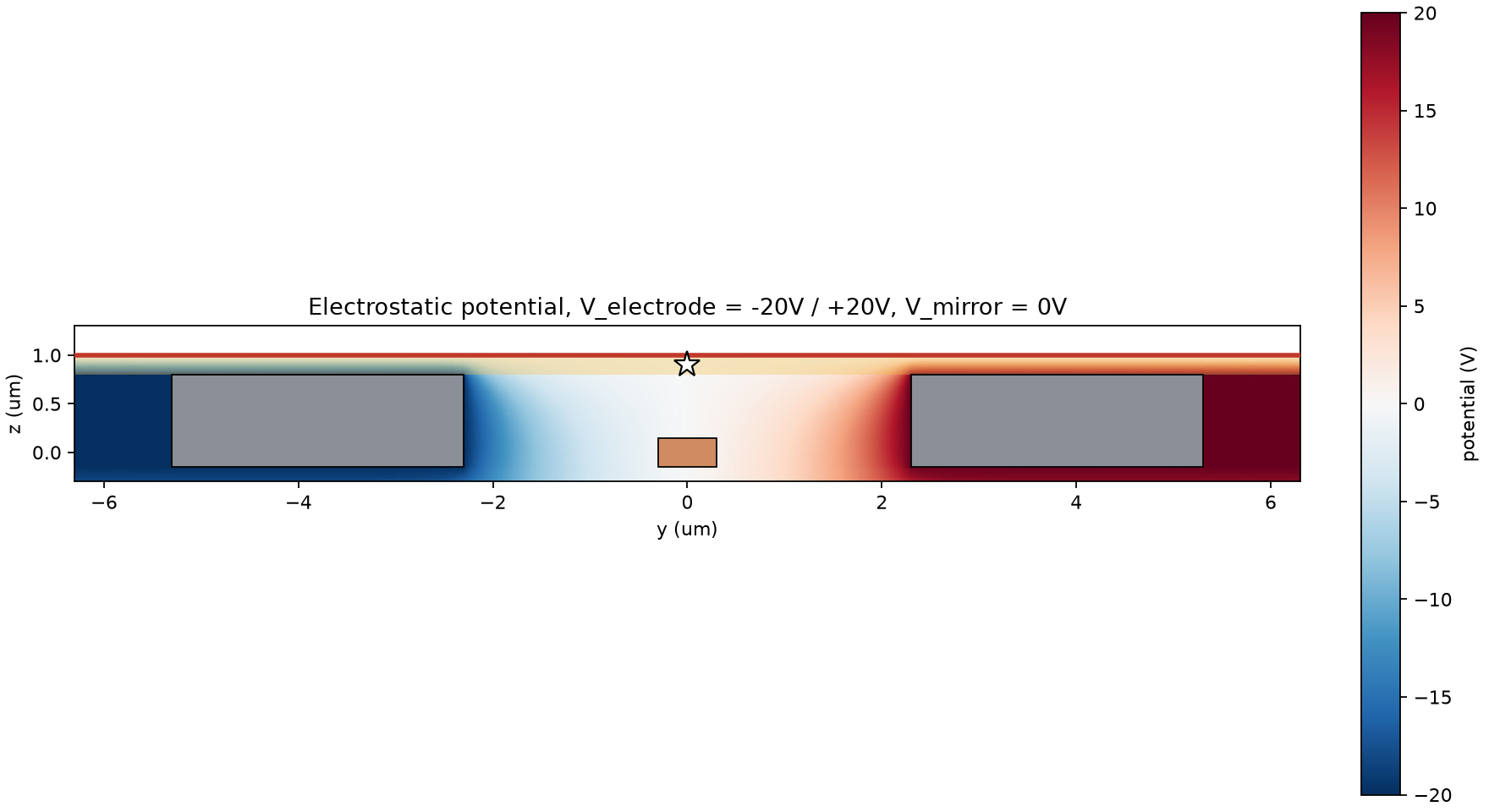
Potential distribution for the same case, sanity-checks the boundary conditions visually.
Both Ey and Ez are reported (task's "go further" option) rather than just |E|, but see the transition-dipole caveat below.
Sanity checks that passed
- V(molecule) = 0 for symmetric differential drive at y = 0, as expected.
- Doubling the mesh density changes the molecule field by < 1%.
- The field response is exactly linear in drive voltage (as it must be for a linear PDE with no space charge).
Converting to a Stark shift (not done)
We were asked to convert E-field-per-volt into a frequency shift (GHz/V) if we could. We did not attempt this: it requires DBT:anthracene's permanent-dipole-moment difference between ground and excited state (Delta-mu), which we don't have a reliable value for and were not willing to make up. If the PI has a Delta-mu value (from spectral-hole-burning Stark spectroscopy on DBT:anthracene, for example), the conversion is Delta-f = (Delta-mu . E) / h, i.e. straightforward given that number and the E-field values reported here.
Open questions / caveats for the PI
- Interpretation of the z-stack (see above) -- please confirm the mirror-bonded-to-crystal picture matches the intended fab process, or correct it (e.g. if there's an air gap between crystal and mirror, that would reduce the field at the molecule and should be re-run).
- Anthracene DC dielectric constant is a placeholder (3.2, ~n^2) -- not a literature-cited measurement. Low confidence flagged explicitly above.
- Waveguide width (0.6 um) and electrode gap (2 um) are assumptions, not taken from the v3 README or GDS -- please confirm against the actual Stark-electrode GDS layout once it exists.
- Transition dipole axis is not mapped to (y, z). We report Ey and Ez separately, but connecting either to the molecule's actual transition dipole direction requires knowing how the anthracene crystal's crystallographic axes are oriented relative to the chip's y/z axes in the stamped/bonded orientation, which isn't specified anywhere we could find. Currently Ey (in-plane, electrode-driven) dominates by ~4-5 orders of magnitude over Ez, so the electrodes are doing essentially all the tuning work in this geometry regardless of exact dipole orientation, but the projected (dipole-aligned) field could be smaller than the reported |E| if the dipole isn't well-aligned with y.
- This is a 2D (translationally-invariant-in-x) approximation. The real geometry has finite extent along the waveguide-propagation direction (crystal thickness, mirror standoff); a full 3D solve would capture x-direction fringing that this cross-section can't.
- Field-map color scale caveat (electrode-corner singularity) noted above -- don't read 118 MV/m as a real number anywhere in the device.
Files
solver.py        geometry, mesh, FEM assembly, solve_potential()/molecule_field()
run_sweep.py      21-point voltage sweep + field-map case + mesh convergence check -> data/
make_figures.py   field map, potential map, E-vs-V plot -> figures/
data/
  sweep_results.npz   V_sweep, Ey, Ez, Emag, Vmol at the molecule, linear fit
  fieldmap_case.npz   full mesh + phi/Ey/Ez/E_mag for the +/-20V case (for plotting)
figures/
  field_map.png       |E| map, full domain, geometry annotated
  field_map_zoom.png  |E| map, zoomed to waveguide/gap/crystal region
  potential_map.png   potential map, same case
  field_vs_voltage.png  the core Stark-tuning-per-volt result
Run
cd electronics_electrostatics/v3_stark_tuning
../../.venv/bin/python run_sweep.py     # ~25s, writes data/
../../.venv/bin/python make_figures.py  # writes figures/
solver.py can also be used standalone:
from solver import molecule_field
molecule_field(V_mirror=0.0, V_electrode_left=-10.0, V_electrode_right=10.0)
# -> {'y_m', 'z_m', 'V', 'Ey_V_per_m', 'Ez_V_per_m', 'E_mag_V_per_m'}
Source: electronics_electrostatics/v3_stark_tuning/