Crystal transition (supplemental)
Supplemental Tidy3D study of the crystal transition region.
No top-level README -- this is the most complete of four dated Tidy3D runs under results/; the other three (20260507_120157, 20260507_120406, 20260507_122710) cover earlier parameter choices.
Generated: 2026-05-07T12:29:37
Purpose
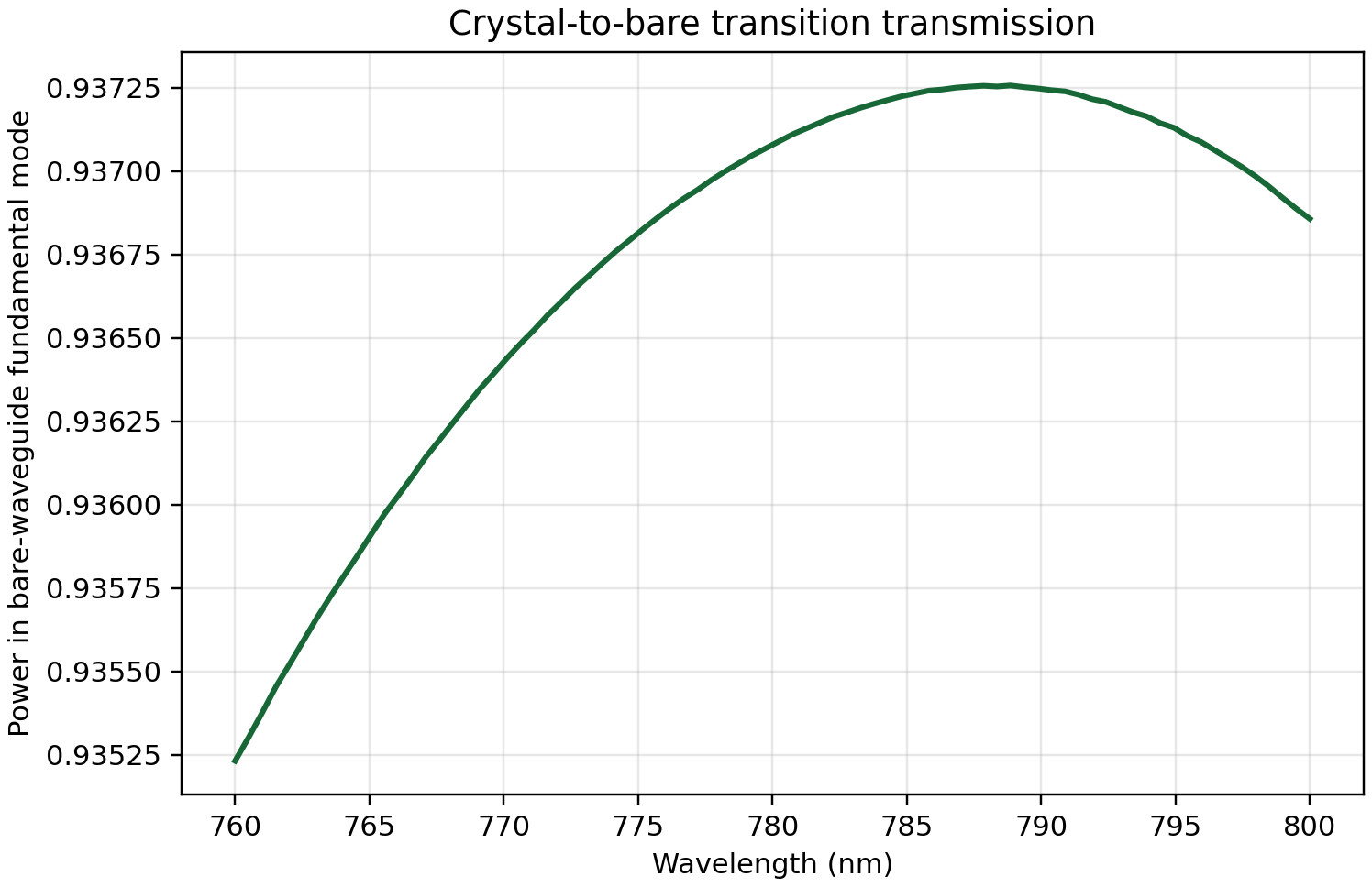
Estimate power coupled from the fundamental TE-like mode of a crystal-covered Si3N4 waveguide into the fundamental TE-like mode of the corresponding bare PVA-clad Si3N4 waveguide across an abrupt transition.
Geometry and Materials
- Coordinates: x is propagation, y is lateral, z is vertical.
- The Si3N4 waveguide center is at z=0.
- Wavelength sweep: 760.0-800.0 nm with center 780.0 nm.
- Si3N4 waveguide: 450.0 nm wide, 300.0 nm thick, n=2.
- SiO2 substrate: thickness 1.2 um, n=1.45.
- PVA cladding: n=1.5.
- Crystal: 200.0 nm thick, full lateral simulation width, n=1.8.
- Simulation size: 10 um x 4 um x 3 um.
- Source x: -3 um; output mode monitor x: 3 um.
Geometry Plots
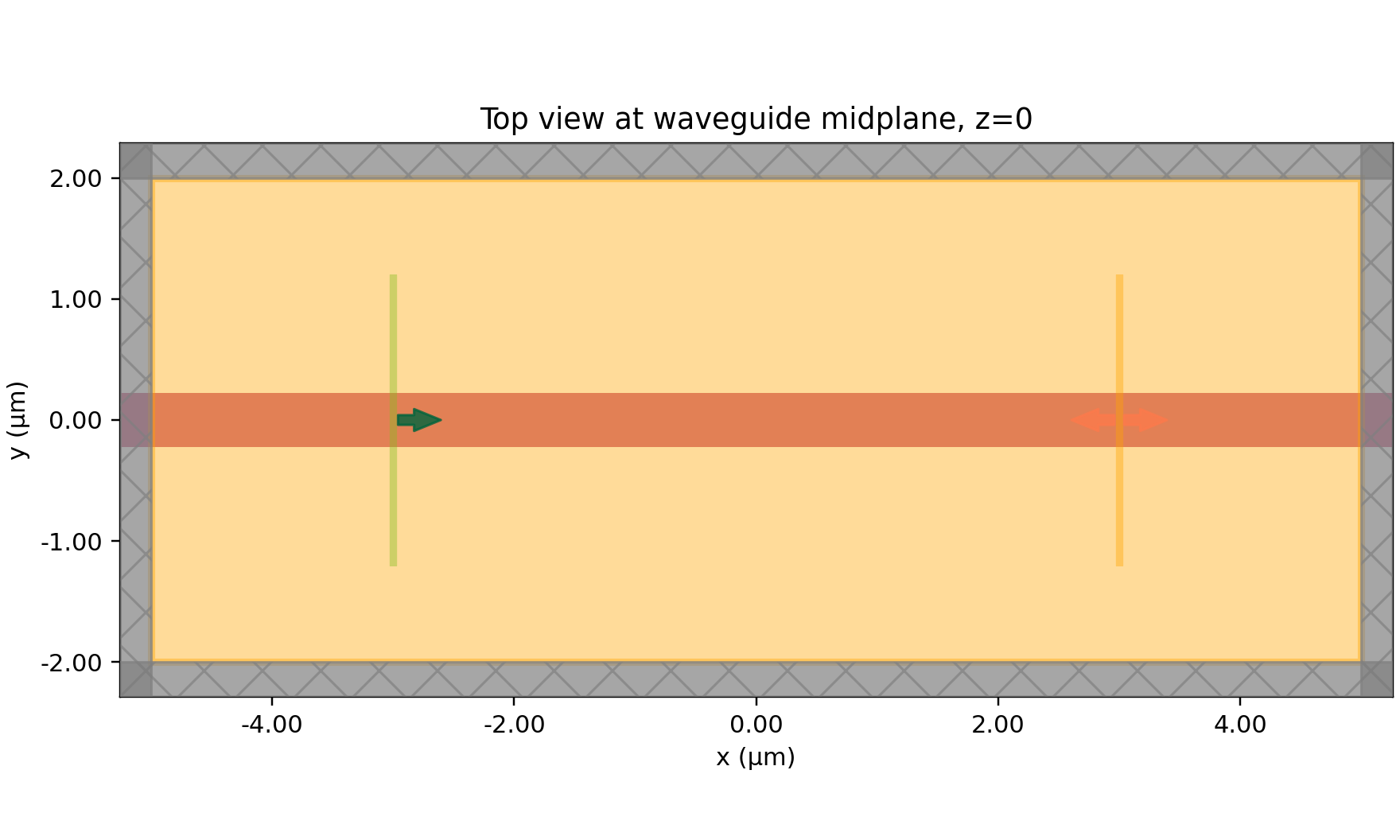
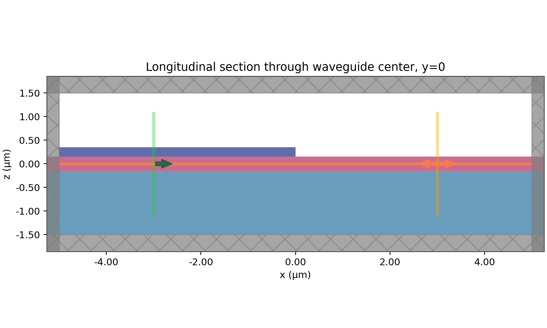
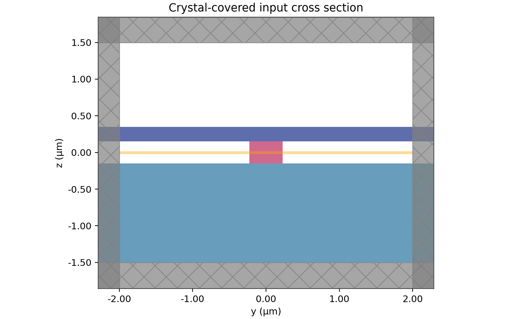
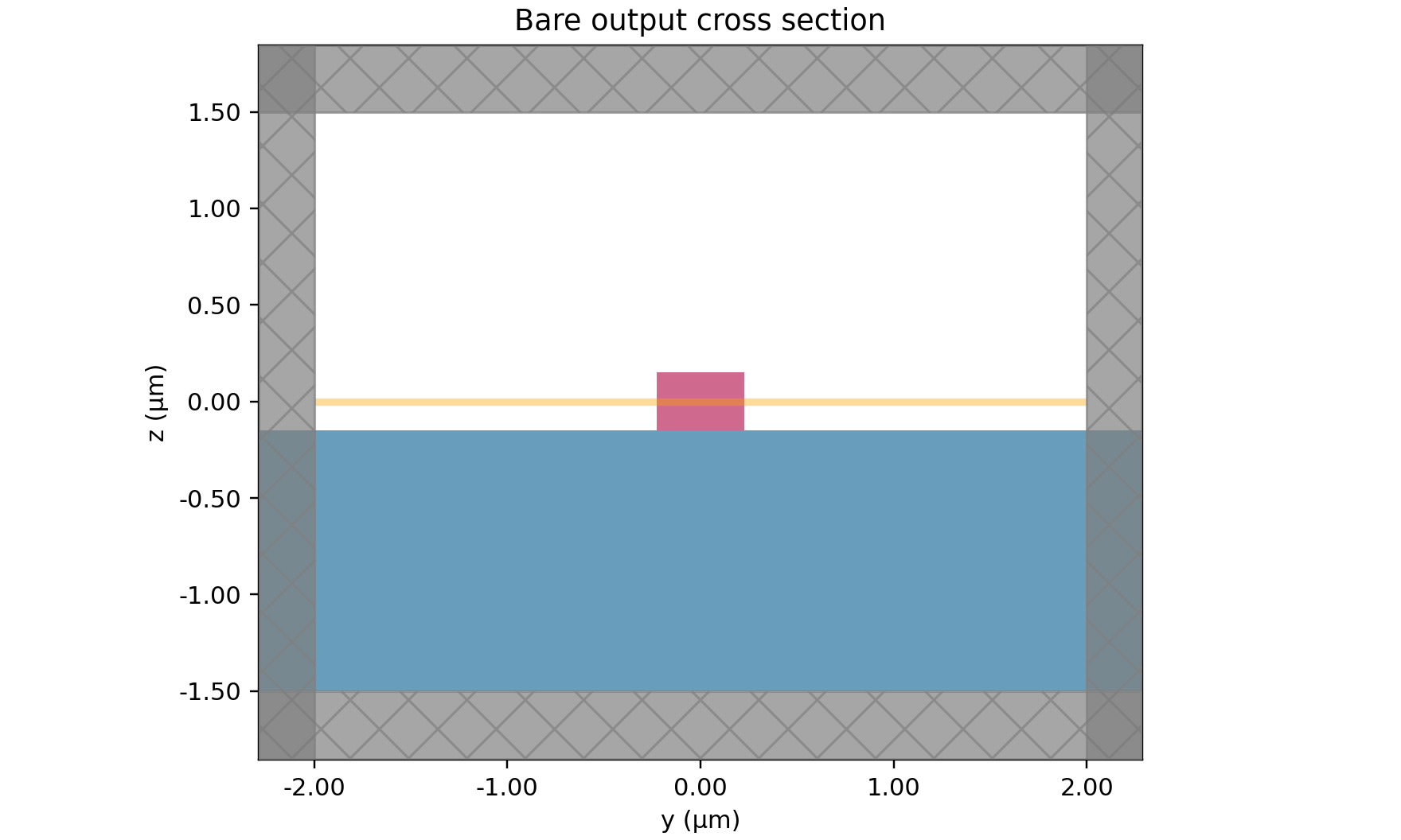
Mode Profiles
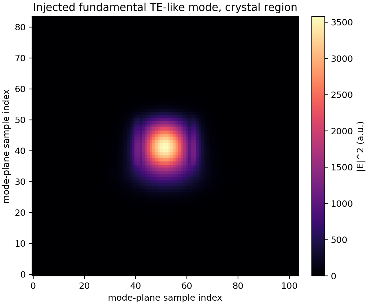
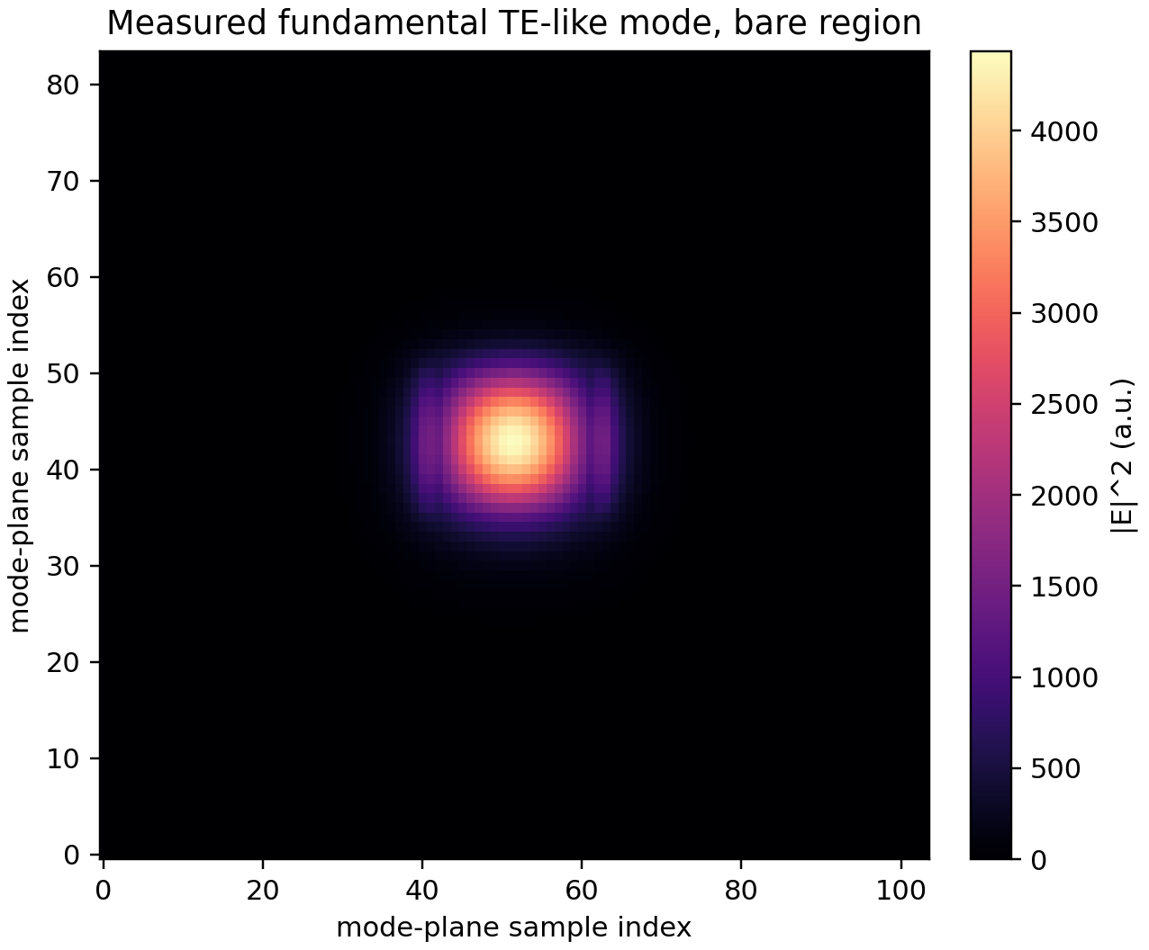
The mode profiles are local eigenmode solves at the source plane in the crystal-covered region and at the output monitor plane in the bare region.
FDTD Results
Downloaded simulation data: simulation_data.hdf5
Reproducibility
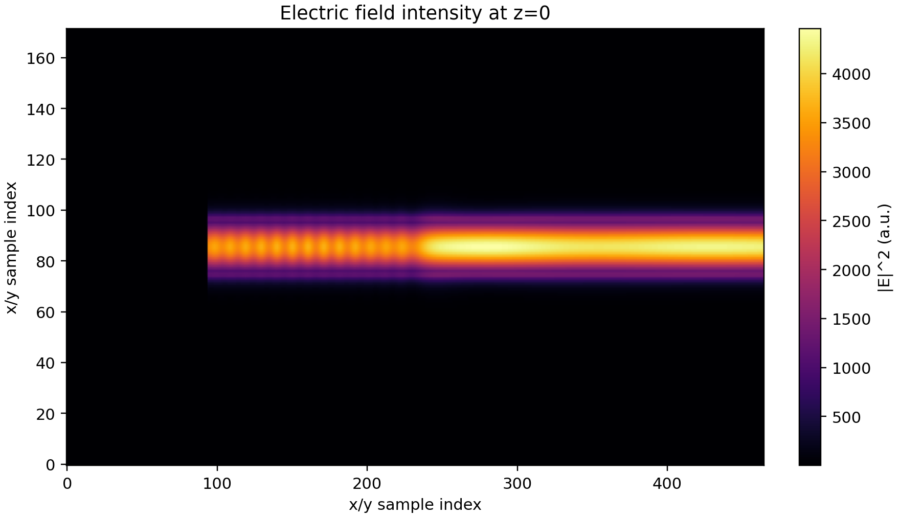
The script builds one 3D FDTD simulation with an abrupt crystal step at x=0. All material models are nondispersive constants unless CLI overrides are supplied.
Downloads
FDTD simulation study only -- no GDS/STL deliverable files exist in this tree.
Source: nanophotonic_devices/emitter_coupling/crystal_transition_supplemental_v1/