In-plane photon extractor
Parametrized in-plane light-extractor package (geometry/materials/monitors/optimizer CLI) with baseline configs and swept runs.
No top-level README -- this package has no single project writeup; each optimizer run under configs/runs/ writes its own notebook.md. Shown below is the latest full baseline run.
- Run ID:
2026-05-17_21-35-45__baseline__si3n4base-0__si3n4total-300__si3n4opt-300__anth-200-bottom__cap-pva__full - Mode:
full(30 iterations) - Started: 2026-05-17T21:35:45
- Wavelength: 780.0 nm
- Output dir:
runs\2026-05-17_21-35-45__baseline__si3n4base-0__si3n4total-300__si3n4opt-300__anth-200-bottom__cap-pva__full
Configuration
name = 'baseline'
mode = 'full'
seed = 0
wl_um = 0.78  # um - central wavelength
bw_um = 0.02  # um - spectral monitor bandwidth
n_wl = 21
n_sub = 1.44  # SiO2 substrate index
t_si3n4_total_nm = 300  # nm - total Si3N4 thickness: base + optimization
t_si3n4_base_nm = 0  # nm - uniform Si3N4 film below optimization region
n_si3n4 = 2.0  # Si3N4 index
cr_l_um = 5.0  # um - design region length (x)
cr_w_um = 3.0  # um - design region width (y)
grid_size_um = 0.04  # um - design grid pitch
min_feature_um = 0.16  # um - fabrication minimum feature
wg_width_um = 0.45  # um - waveguide width
wg_length_um = 1.5  # um - waveguide lead-in length
wg_crossbar = False  # fixed transverse Si3N4 bar at design-region input
wg_crossbar_width_nm = 100  # nm - x-width of fixed input cross bar
t_anth_nm = 200  # nm - anthracene crystal thickness
n_anth = 1.8  # anthracene index
qe_z_position = 'bottom'
cap_material = 'pva'
n_pva = 1.44  # PVA index
t_pva_nm = 1000.0  # nm - PVA capping thickness
n_alox = 1.65  # Al2O3 index
t_alox_nm = 10.0  # nm - Al2O3 capping thickness
cap_mesh_min_cells = 2  # cells - minimum z mesh cells through non-air cap
qe_x_um = 0.0  # um - QE x-position relative to design-region center
dipole_polarization = 'Ey'
learning_rate = 0.1
beta_min = 1.0
iter_steps = 2
penalty_weight = 0.1
flux_report_interval = 5  # iterations - side-flux reporting interval; 0 disables
output_root = 'runs'
verbose = True
t_si3n4_nm = 300  # nm - derived optimization Si3N4 thickness
Layer stack
| Layer | n | z_bottom (nm) | z_top (nm) | thickness (nm) |
|---|---|---|---|---|
| SiO2 substrate | 1.440 | -inf | 0 | inf |
| Si3N4 (uniform base film) | 2.000 | 0.0 | 0.0 | 0.0 |
| Si3N4 (optimization slab) | 2.000 | 0.0 | 300.0 | 300.0 |
| Anthracene crystal | 1.800 | 300.0 | 500.0 | 200.0 |
| Cap (PVA) | 1.440 | 500.0 | 1500.0 | 1000.0 |
| Air | 1.000 | 1500.0 | +inf | inf |
Quantum emitter (Ey dipole) at x = 0.000 um, z = 320.0 nm (bottom of anthracene).
Geometry cross sections
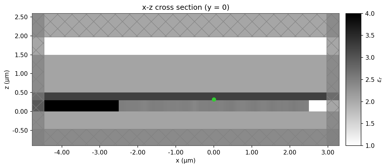
x-z (y = 0)
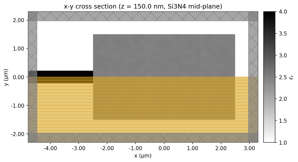
x-y (Si3N4 mid-plane)
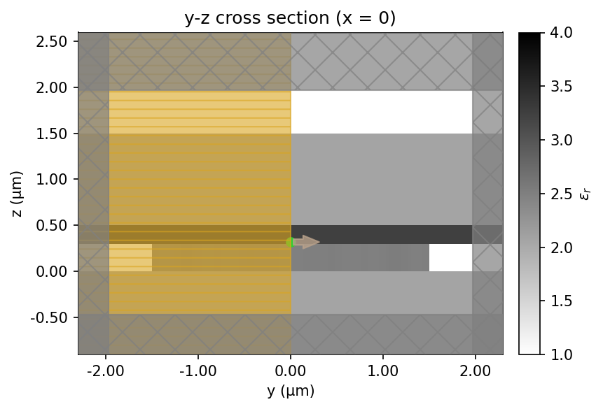
y-z (x = 0)
Objective function
Maximize the coupling efficiency from the dipole emission into the fundamental Si3N4 waveguide mode, subtracting an erosion-dilation fabrication penalty:
$$ J(\rho, \beta) = \frac{|a_{-,0}|2}{\sum_{s=1}(\tilde\rho_\beta) $$} |\Phi_s|} - \lambda_p \cdot \mathrm{ED
where $a_{-,0}$ is the backward fundamental-mode amplitude on the waveguide cross section, $\Phi_s$ is the time-averaged Poynting flux through each of the six surfaces enclosing the dipole, $\tilde\rho_\beta$ is the conic-filtered + tanh-projected density, and $\lambda_p$ is the penalty weight.
Optimization Progress
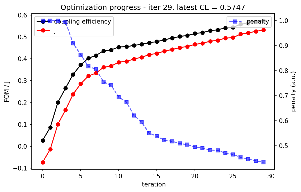
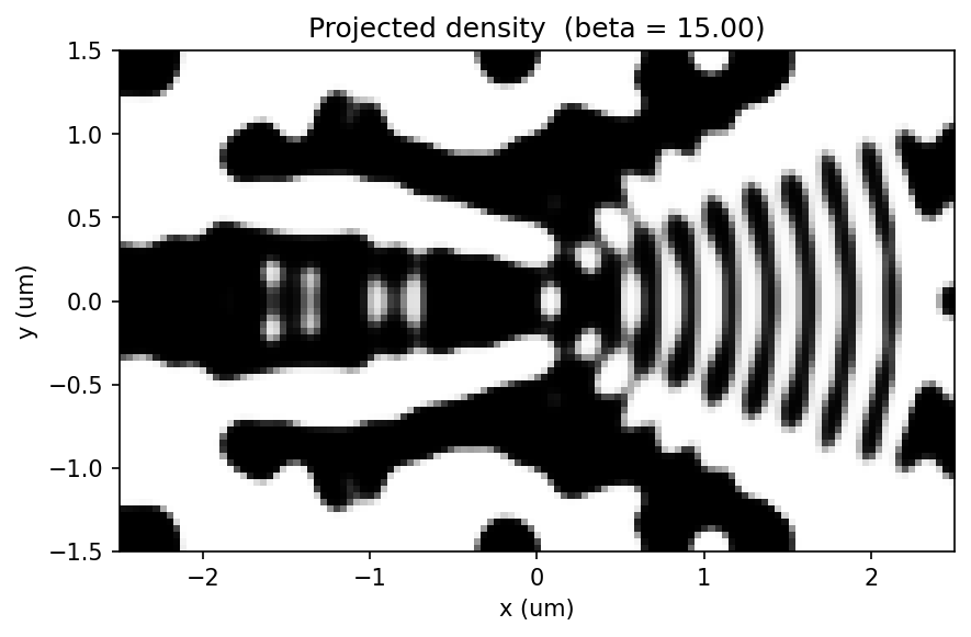
Latest density (iter 29, beta = 15.00):
| iter | beta | J | mode_power | dip_power | coup_eff | penalty |
|---|---|---|---|---|---|---|
| 0 | 1.00 | -7.2970e-02 | 1.158e+02 | 4.283e+03 | 0.0270 | 1.0000 |
| 1 | 1.00 | -1.3750e-02 | 3.725e+02 | 4.318e+03 | 0.0862 | 1.0000 |
| 2 | 2.00 | 1.0067e-01 | 8.769e+02 | 4.370e+03 | 0.2007 | 0.9999 |
| 3 | 2.00 | 1.6574e-01 | 1.163e+03 | 4.385e+03 | 0.2653 | 0.9952 |
| 4 | 3.00 | 2.3800e-01 | 1.482e+03 | 4.504e+03 | 0.3289 | 0.9092 |
| 5 | 3.00 | 2.8565e-01 | 1.716e+03 | 4.613e+03 | 0.3720 | 0.8640 |
| 6 | 4.00 | 3.2113e-01 | 1.882e+03 | 4.671e+03 | 0.4029 | 0.8173 |
| 7 | 4.00 | 3.3455e-01 | 1.913e+03 | 4.608e+03 | 0.4151 | 0.8051 |
| 8 | 5.00 | 3.6105e-01 | 1.985e+03 | 4.546e+03 | 0.4366 | 0.7555 |
| 9 | 5.00 | 3.6666e-01 | 2.002e+03 | 4.543e+03 | 0.4408 | 0.7410 |
| 10 | 6.00 | 3.8465e-01 | 2.116e+03 | 4.661e+03 | 0.4540 | 0.6939 |
| 11 | 6.00 | 3.8834e-01 | 2.175e+03 | 4.773e+03 | 0.4558 | 0.6741 |
| 12 | 7.00 | 3.9898e-01 | 2.211e+03 | 4.796e+03 | 0.4611 | 0.6209 |
| 13 | 7.00 | 4.0743e-01 | 2.255e+03 | 4.831e+03 | 0.4668 | 0.5933 |
| 14 | 8.00 | 4.1896e-01 | 2.368e+03 | 4.996e+03 | 0.4739 | 0.5499 |
| 15 | 8.00 | 4.2458e-01 | 2.524e+03 | 5.276e+03 | 0.4783 | 0.5373 |
| 16 | 9.00 | 4.3515e-01 | 2.702e+03 | 5.546e+03 | 0.4873 | 0.5211 |
| 17 | 9.00 | 4.4268e-01 | 2.876e+03 | 5.817e+03 | 0.4944 | 0.5173 |
| 18 | 10.00 | 4.5129e-01 | 3.089e+03 | 6.152e+03 | 0.5021 | 0.5082 |
| 19 | 10.00 | 4.5622e-01 | 3.361e+03 | 6.634e+03 | 0.5066 | 0.5041 |
| 20 | 11.00 | 4.6612e-01 | 3.711e+03 | 7.197e+03 | 0.5156 | 0.4948 |
| 21 | 11.00 | 4.7092e-01 | 4.067e+03 | 7.823e+03 | 0.5199 | 0.4902 |
| 22 | 12.00 | 4.8068e-01 | 4.219e+03 | 7.977e+03 | 0.5289 | 0.4822 |
| 23 | 12.00 | 4.8447e-01 | 4.514e+03 | 8.477e+03 | 0.5326 | 0.4809 |
| 24 | 13.00 | 4.9476e-01 | 4.360e+03 | 8.047e+03 | 0.5418 | 0.4700 |
| 25 | 13.00 | 4.9702e-01 | 4.811e+03 | 8.851e+03 | 0.5435 | 0.4650 |
| 26 | 14.00 | 5.1288e-01 | 4.702e+03 | 8.423e+03 | 0.5582 | 0.4530 |
| 27 | 14.00 | 5.1820e-01 | 4.840e+03 | 8.599e+03 | 0.5628 | 0.4465 |
| 28 | 15.00 | 5.2574e-01 | 5.095e+03 | 8.943e+03 | 0.5697 | 0.4391 |
| 29 | 15.00 | 5.3135e-01 | 5.116e+03 | 8.903e+03 | 0.5747 | 0.4334 |
Directional flux breakdown
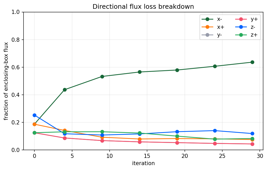
These values are the absolute flux through each enclosing-box side; the percent columns are normalized by the summed six-side flux for that row.
| iter | x- | x+ | y- | y+ | z- | z+ |
|---|---|---|---|---|---|---|
| 0 | 8.023e+02 (18.7%) | 7.989e+02 (18.7%) | 5.329e+02 (12.4%) | 5.329e+02 (12.4%) | 1.082e+03 (25.3%) | 5.344e+02 (12.5%) |
| 4 | 1.966e+03 (43.7%) | 6.363e+02 (14.1%) | 3.904e+02 (8.7%) | 3.904e+02 (8.7%) | 5.287e+02 (11.7%) | 5.923e+02 (13.1%) |
| 9 | 2.420e+03 (53.3%) | 4.185e+02 (9.2%) | 3.074e+02 (6.8%) | 3.074e+02 (6.8%) | 4.908e+02 (10.8%) | 5.990e+02 (13.2%) |
| 14 | 2.823e+03 (56.5%) | 3.963e+02 (7.9%) | 2.924e+02 (5.9%) | 2.924e+02 (5.9%) | 5.801e+02 (11.6%) | 6.117e+02 (12.2%) |
| 19 | 3.844e+03 (57.9%) | 5.475e+02 (8.3%) | 3.507e+02 (5.3%) | 3.507e+02 (5.3%) | 8.770e+02 (13.2%) | 6.644e+02 (10.0%) |
| 24 | 4.881e+03 (60.6%) | 6.485e+02 (8.1%) | 3.805e+02 (4.7%) | 3.805e+02 (4.7%) | 1.127e+03 (14.0%) | 6.303e+02 (7.8%) |
| 29 | 5.665e+03 (63.6%) | 6.693e+02 (7.5%) | 3.871e+02 (4.3%) | 3.871e+02 (4.3%) | 1.057e+03 (11.9%) | 7.375e+02 (8.3%) |
Final results
The final broadband simulation uses the thresholded binary design saved for GDS export. Optimization-progress coupling values are measured on the continuous filtered design at that iteration, so they are not always identical to the final binary-design metric.
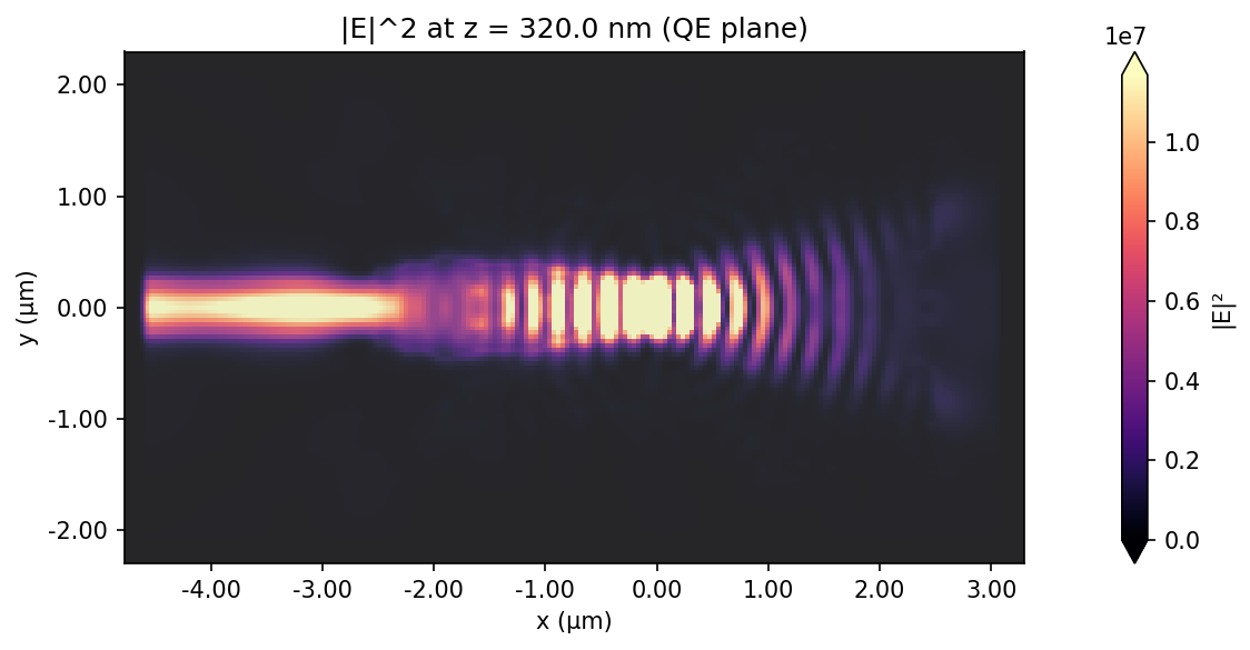
Final |E|^2 - xy
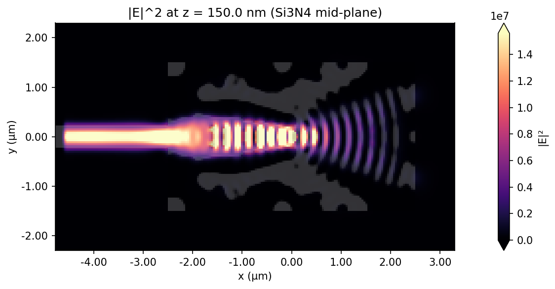
Final |E|^2 - xy_si3n4
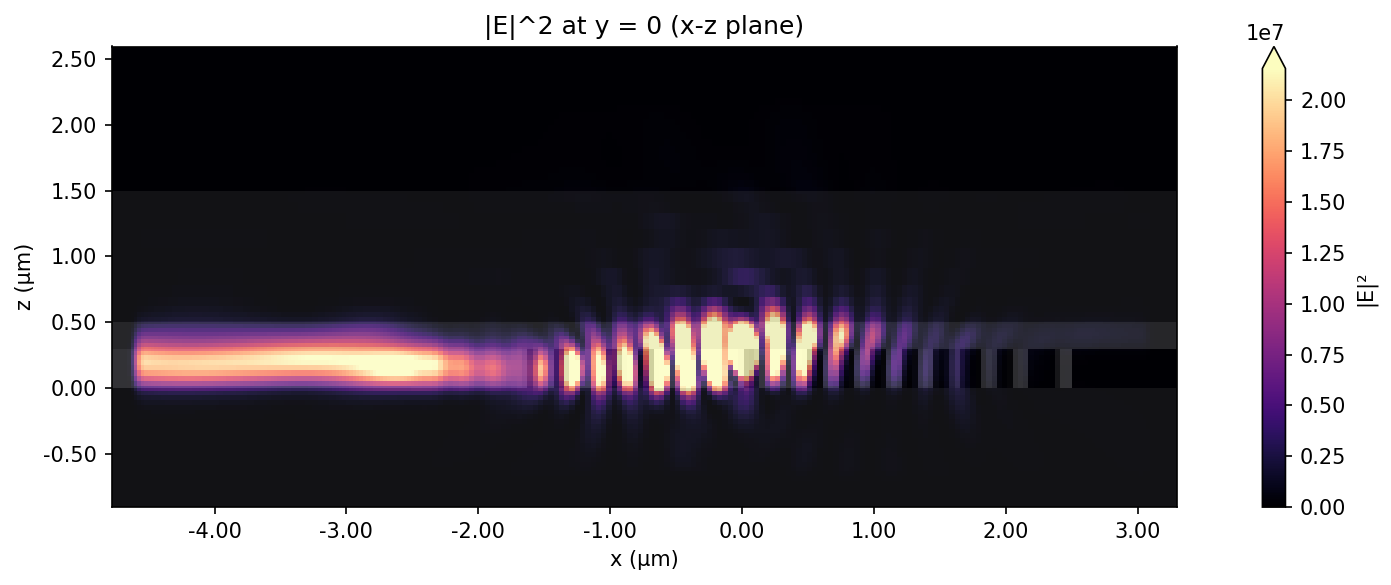
Final |E|^2 - xz
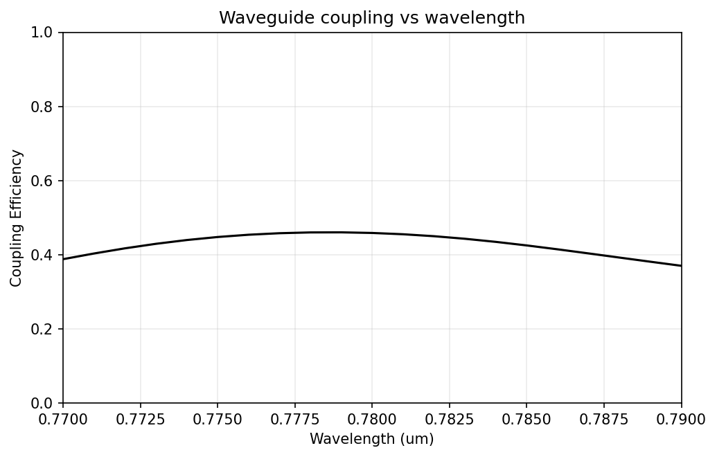
Final coupling efficiency vs wavelength
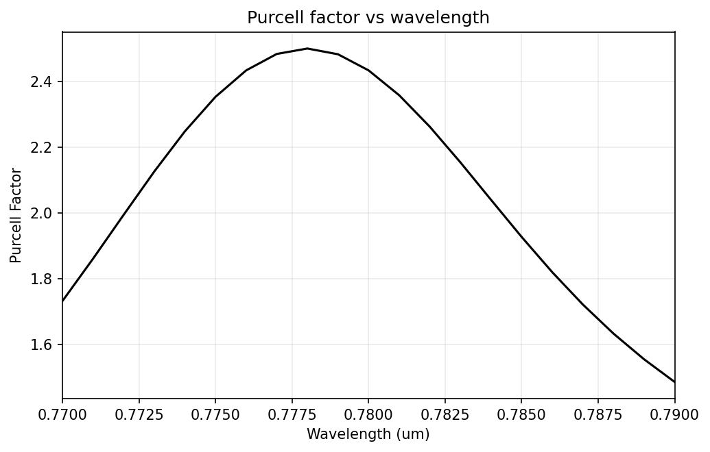
Final Purcell factor vs wavelength
At 780.0 nm: coupling efficiency = 0.4587, Purcell factor = 2.4329. Underlying arrays are saved in spectral_metrics.npz.
GDS file: final_design.gds (threshold eps = 2.500, sliced at z = 150.0 nm)
Best iteration: 29 (J = 5.3135e-01, coupling eff = 0.5747, beta = 15.00)
Run summary
- Run directory:
runs\2026-05-17_21-35-45__baseline__si3n4base-0__si3n4total-300__si3n4opt-300__anth-200-bottom__cap-pva__full - Mode:
full(30 iterations)
Run completed after 1889.9 s.
Downloads
6 GDS exports total exist across configs/runs/ (one per completed optimizer run); only the latest is linked here.
Source: nanophotonic_devices/gratings_extractors/photon_extractor_in_plane_v1/