Coupling-chip inverse design v2
Two-chip vertical coupler: PEC+crystal mirror chip, and an inverse-designed free-form coupler on the waveguide chip.
Two-chip vertical coupler study. Mirror chip: PEC + anthracene crystal. Coupling chip: free-form inverse-design coupler + solid high-index waveguide.
Stack (bottom → top):
PEC (z- boundary)
  └─ 100 nm anthracene crystal (dipole at mid-plane, 780 nm)
       └─ inverse-design region (xz-plane topology 3×3 µm, y-thickness = waveguide H)
            └─ solid TiO2 waveguide 300×300 nm (propagation +z)
Objective: maximize coupling efficiency into the fundamental guided mode (guided mode power / total radiated power). Long-term target: > 90%.
This package produces a dry-run report only by default. No billed Tidy3D FDTD solve is submitted unless you explicitly approve and launch an optimization or single-shot run later.
Workflow
- Generate the dry-run report (geometry, mode analysis, schematics). No cloud cost estimate unless requested:
- Optionally request non-billed FlexCredit quotes (Tidy3D
estimate_cost; does not start a solver job):
- Review
reports/dry_run_report.html. Do not launch optimization until the projected FlexCredit total is explicitly approved.
Hard rule
Never spend FlexCredits without explicit user permission. This codebase will
not call web.run / optimizer .run from the dry-run path. Optimization entry
points (when added) must refuse to start without an explicit approval flag and
prior cost estimates under threshold.
Results
Silver-mirror baseline
Silver mirror vs PEC — high-η half-clad baseline
Same geometry that gave ~83–89% with ideal PEC:
- Half-clad Si3N4 400×300 nm (SiO₂ for y ≤ −0.15 µm, air above)
- Crystal mid-plane dipole, n = 1.8
- Crystal 50 nm (PEC TE ~89%) and 100 nm (PEC TE ~83.5%)
Only change: PEC → Ag (Johnson–Christy 1972), 200 nm thick, with SiO₂ buffer + PML below.
Billed FlexCredits: 0.2376 FC (estimated sum 2.3765 FC).
Collection efficiency @ 780 nm
| Crystal (nm) | Pol | η Ag (mode) | η Ag (flux) | η PEC (ref) | Δ Ag−PEC (pt) | n_eff | Billed FC |
|---|---|---|---|---|---|---|---|
| 50 | TE (Ex) | 31.95% | 29.90% | 89.0% | -57.1 | 1.6042 | 0.0562 |
| 50 | TM (Ey) | 26.38% | 24.36% | 84.2% | -57.8 | 1.5832 | 0.0562 |
| 100 | TE (Ex) | 34.08% | 31.78% | 83.5% | -49.4 | 1.6042 | 0.0627 |
| 100 | TM (Ey) | 29.84% | 27.41% | 77.2% | -47.4 | 1.5832 | 0.0627 |
η_mode uses the strongest of the first two pol-filtered modes (Ey often lands on mode 1 if unfiltered).
Geometry and |E|
Crystal 50 nm, TE — Ag η = 31.95% (PEC ref 89.0%)
Billed FC: 0.0562.
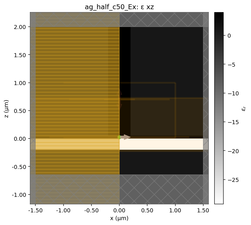
ag_half_c50_Ex geometry x–z (Ag → crystal → WG)
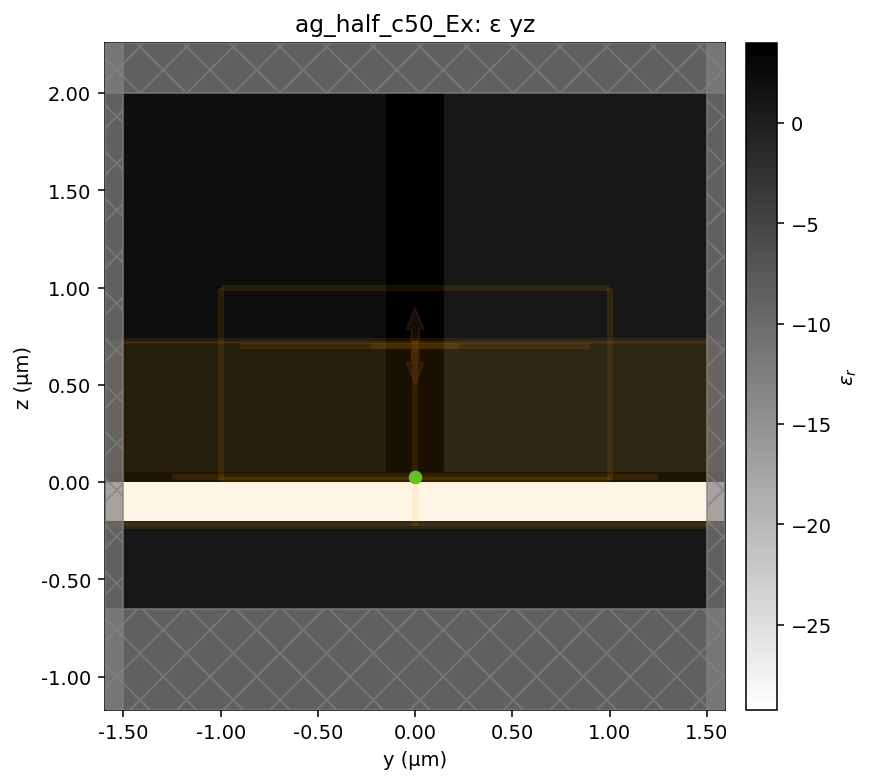
ag_half_c50_Ex geometry y–z (half-clad)
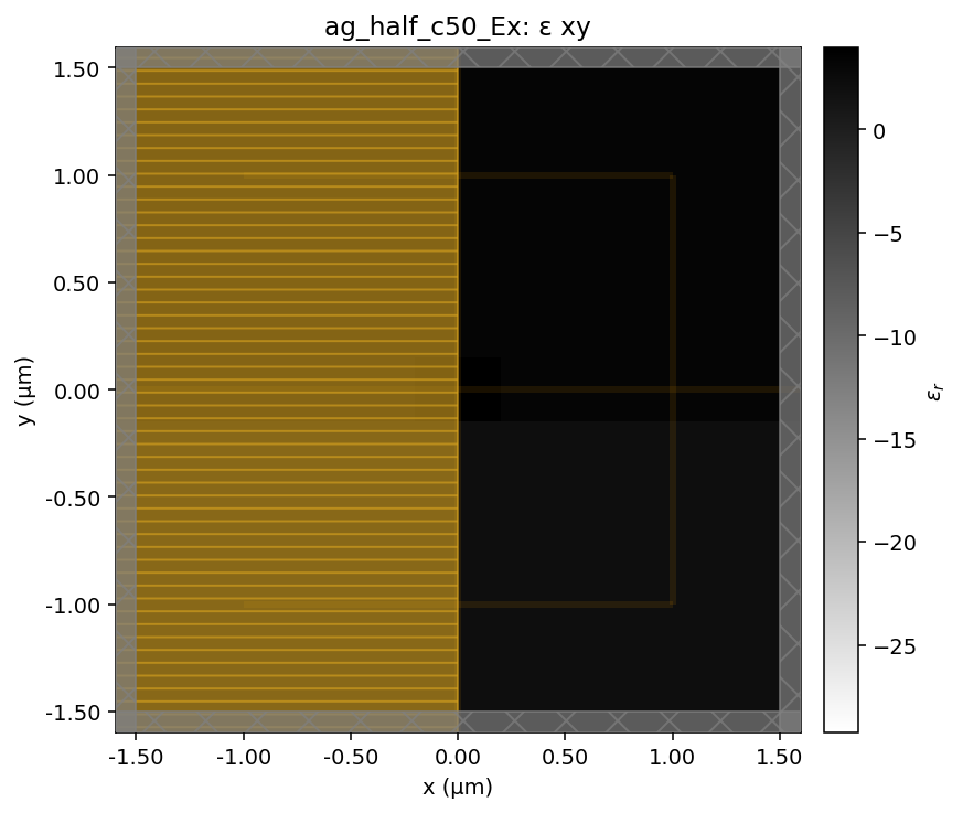
ag_half_c50_Ex geometry x–y
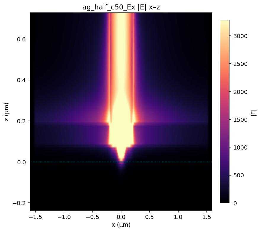
ag_half_c50_Ex |E| x–z
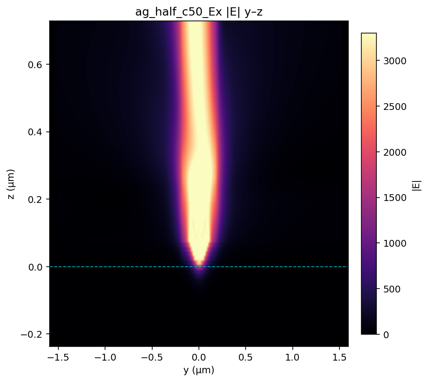
ag_half_c50_Ex |E| y–z
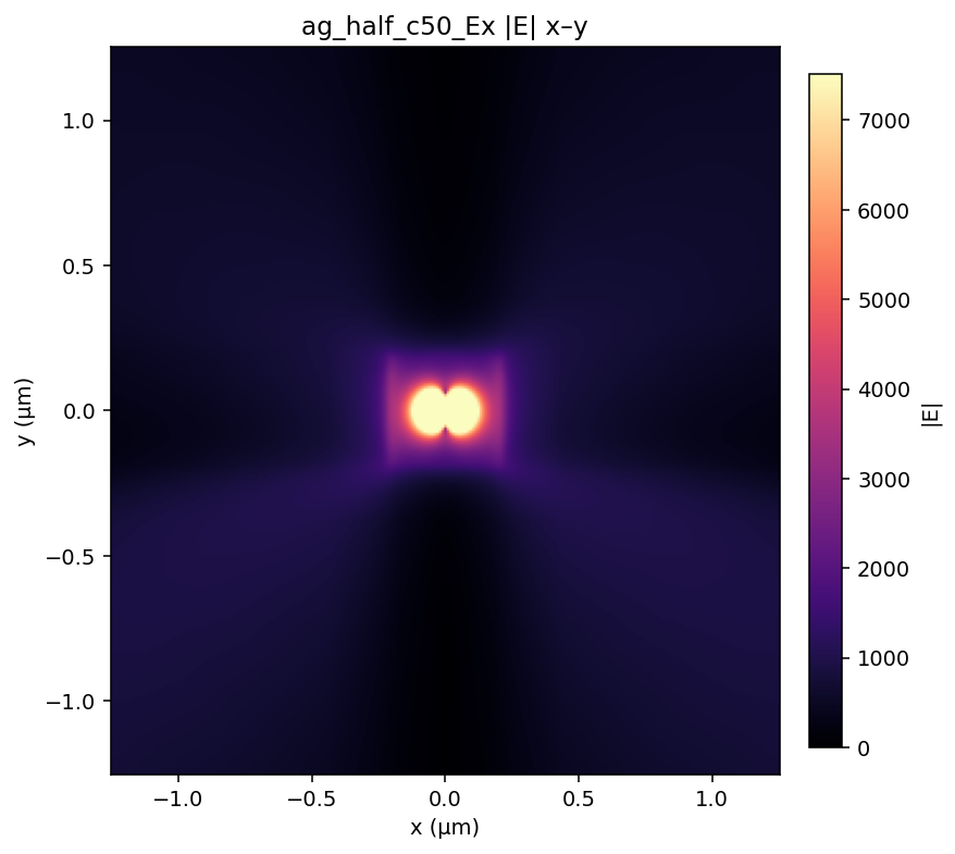
ag_half_c50_Ex |E| x–y
Crystal 50 nm, TM — Ag η = 26.38% (PEC ref 84.2%)
Billed FC: 0.0562.
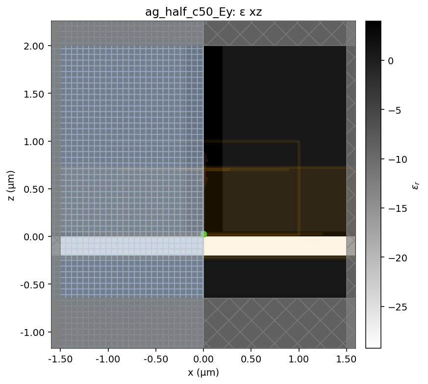
ag_half_c50_Ey geometry x–z (Ag → crystal → WG)
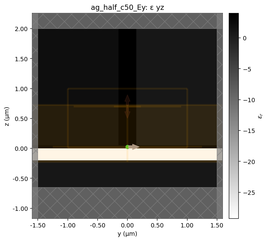
ag_half_c50_Ey geometry y–z (half-clad)
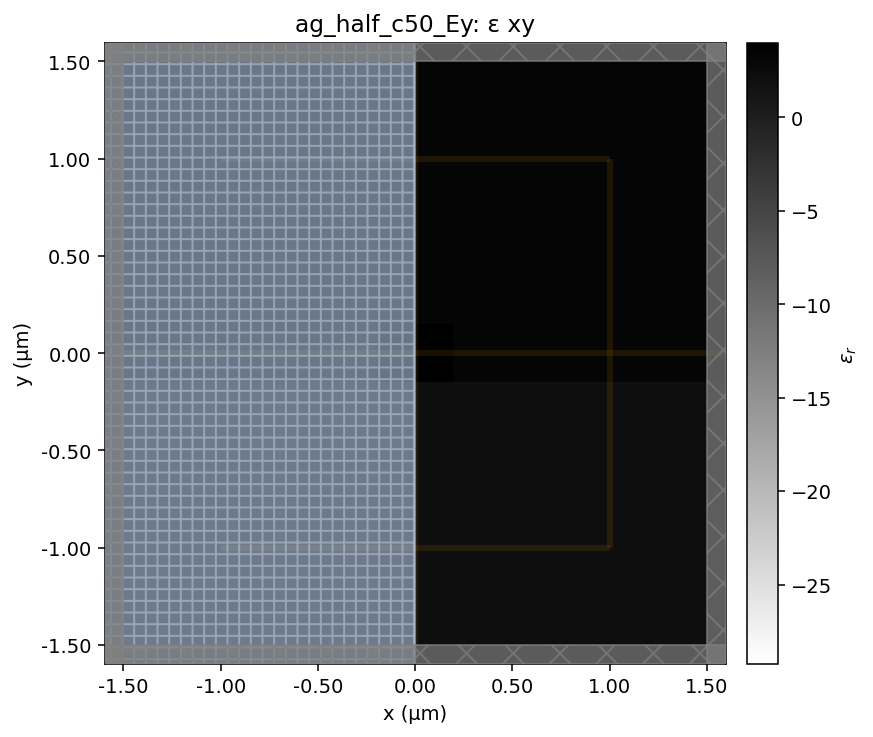
ag_half_c50_Ey geometry x–y
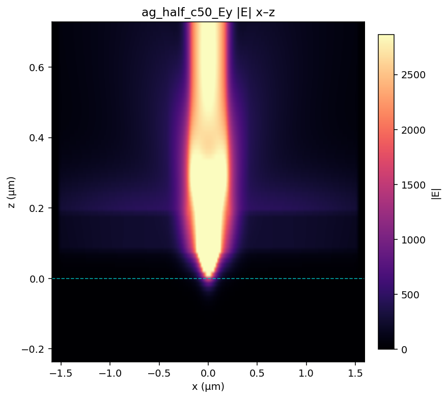
ag_half_c50_Ey |E| x–z
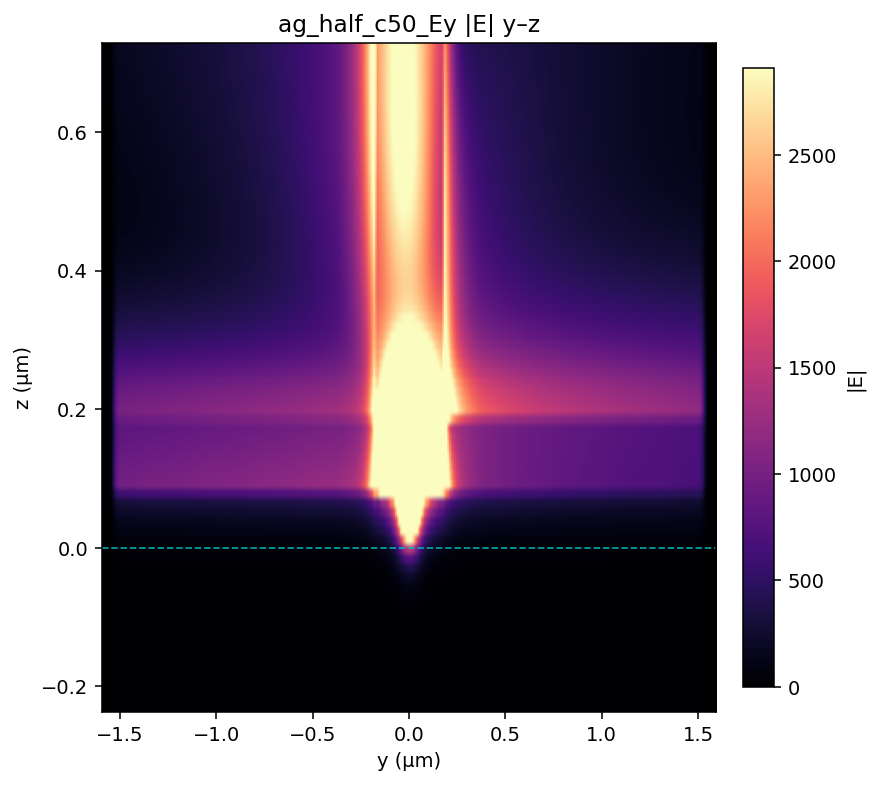
ag_half_c50_Ey |E| y–z
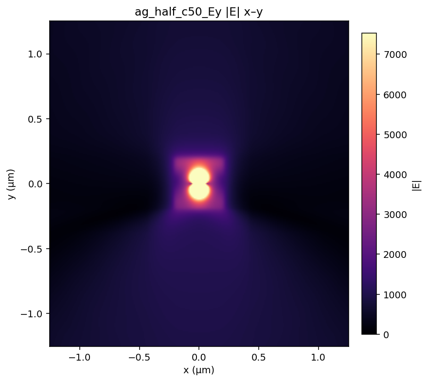
ag_half_c50_Ey |E| x–y
Crystal 100 nm, TE — Ag η = 34.08% (PEC ref 83.5%)
Billed FC: 0.0627.
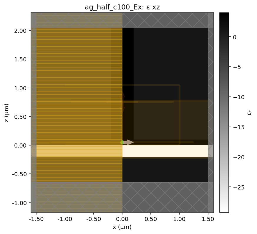
ag_half_c100_Ex geometry x–z (Ag → crystal → WG)
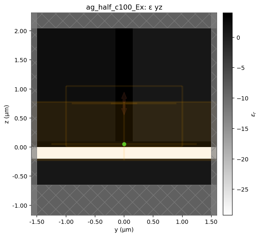
ag_half_c100_Ex geometry y–z (half-clad)
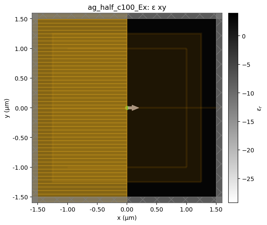
ag_half_c100_Ex geometry x–y
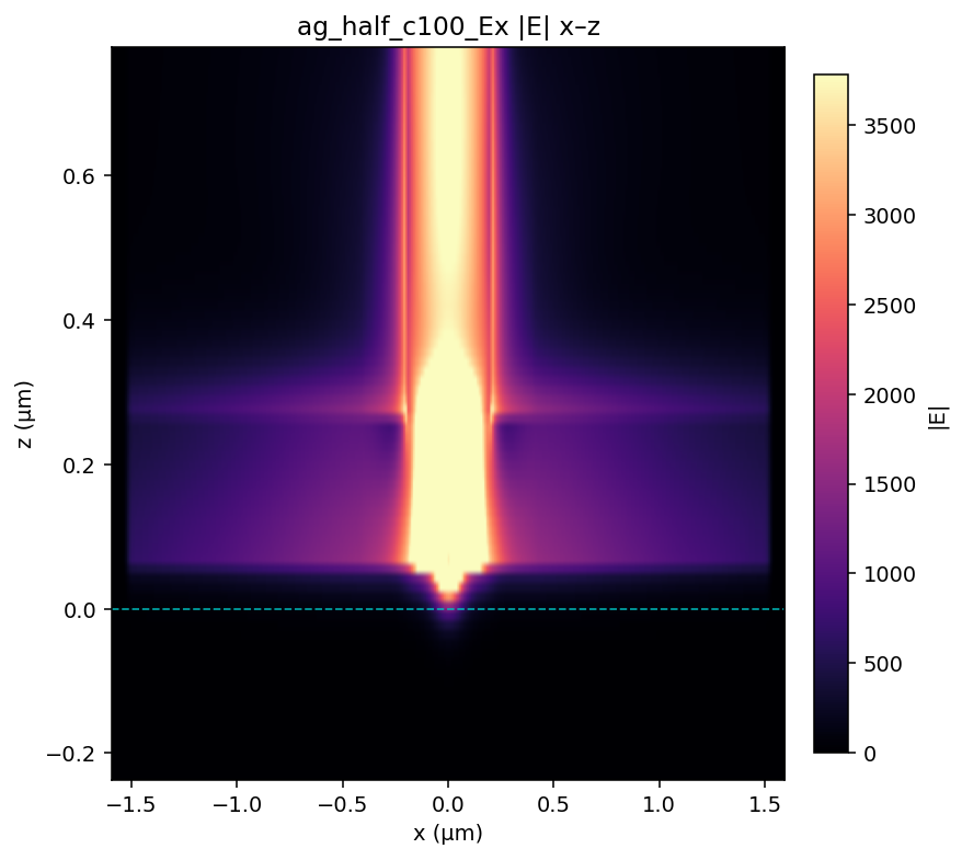
ag_half_c100_Ex |E| x–z
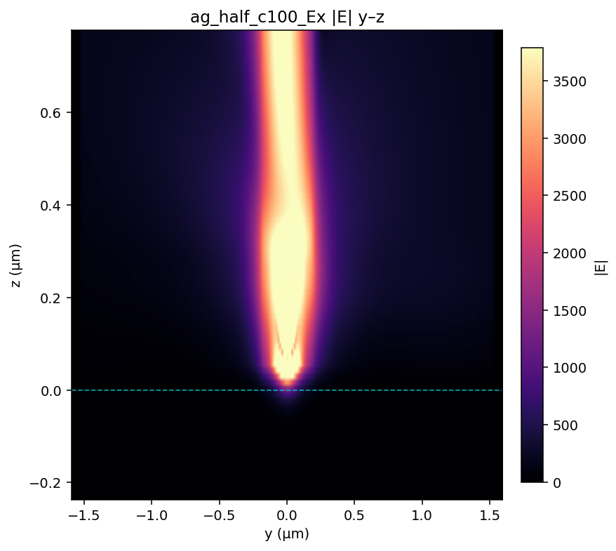
ag_half_c100_Ex |E| y–z
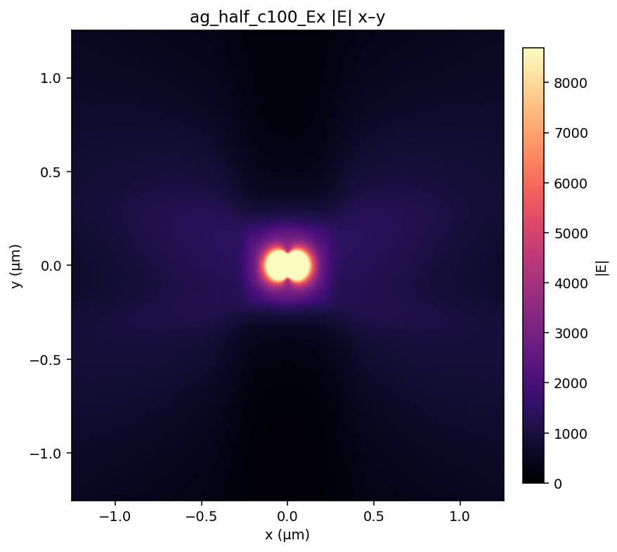
ag_half_c100_Ex |E| x–y
Crystal 100 nm, TM — Ag η = 29.84% (PEC ref 77.2%)
Billed FC: 0.0627.
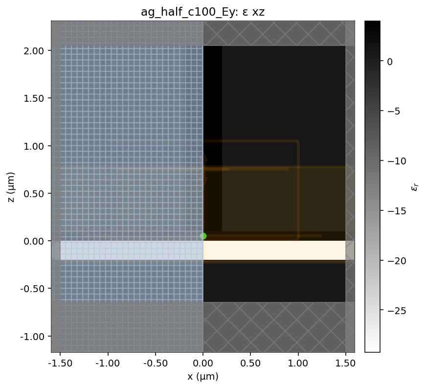
ag_half_c100_Ey geometry x–z (Ag → crystal → WG)
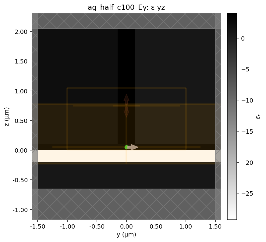
ag_half_c100_Ey geometry y–z (half-clad)
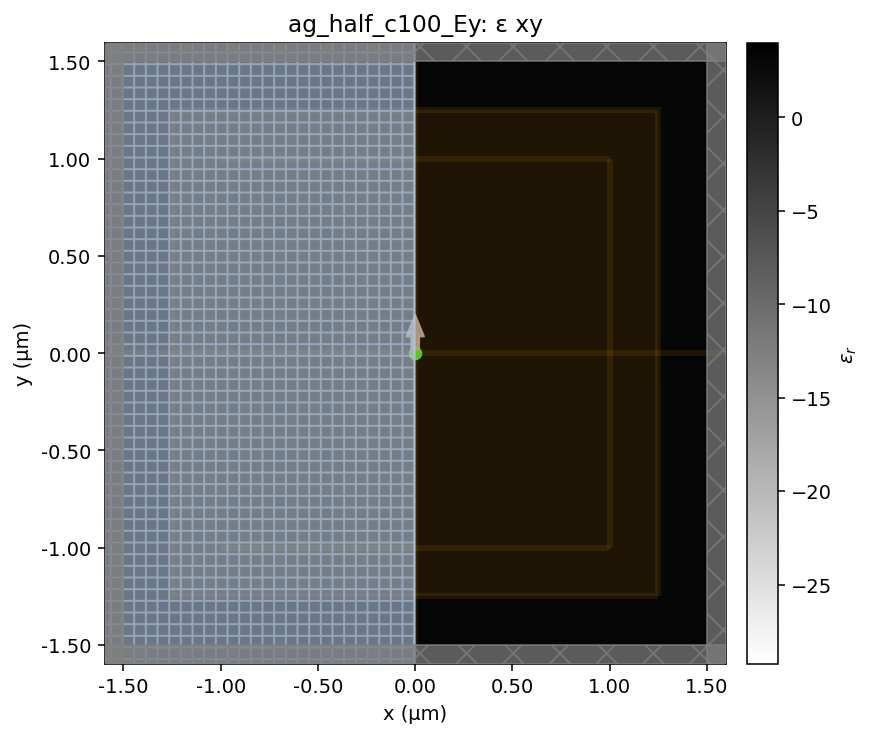
ag_half_c100_Ey geometry x–y
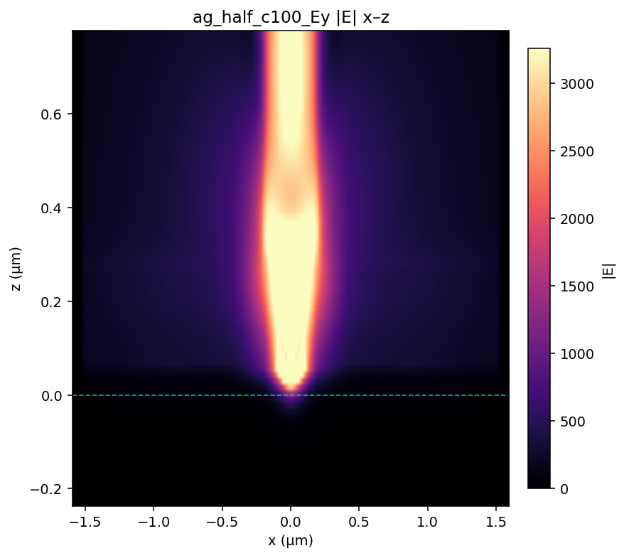
ag_half_c100_Ey |E| x–z
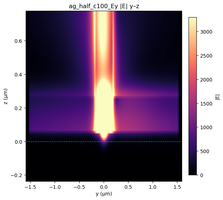
ag_half_c100_Ey |E| y–z
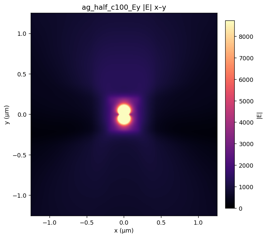
ag_half_c100_Ey |E| x–y
Interpretation
- If Ag η stays within a few points of PEC, real-metal loss is not fatal for this stack.
- Larger drops mean absorption / quenching near Ag (dipole is only 25–50 nm from metal).
- Further optimization: thin dielectric spacer on Ag, or slightly thicker crystal tradeoff.
Metrics: silver_mirror_baseline_metrics.json
Best patch + 100 nm crystal (best result)
Best patch + 100 nm crystal
Patch: PEC circle r = 250 nm, thickness 100 nm (best from size/shape sweep). Crystal: 100 nm, dipole at mid-plane (50 nm from patch top). Waveguide: Si3N4 400×300 nm, full SiO₂ clad. PML all sides.
Results @ 780 nm
| Configuration | TE | TM |
|---|---|---|
| Best patch (r=250) + 100 nm crystal (this run) | 80.66% | 74.21% |
| Best patch (r=250) + 200 nm crystal (prior sweep) | 66.01% | 62.80% |
| Infinite PEC + 100 nm crystal mid (prior full clad) | 77.26% | 71.41% |
| Infinite PEC + 200 nm crystal mid (prior full clad) | 58.39% | 55.30% |
Comparison
- Thinning 200→100 nm on the best patch: TE 66.0% → 80.7% (Δ +14.6 pt); TM 62.8% → 74.2% (Δ +11.4 pt).
- Best patch + 100 nm vs infinite PEC + 100 nm: TE 80.7% vs 77.3% (Δ +3.4 pt); TM 74.2% vs 71.4% (Δ +2.8 pt).
TE — η = 80.66%
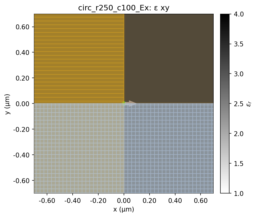
circ_r250_c100_Ex geometry x–y
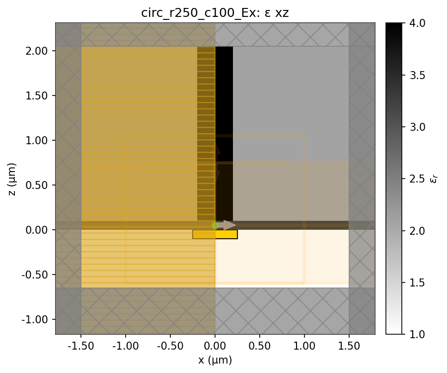
circ_r250_c100_Ex geometry x–z
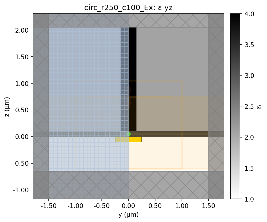
circ_r250_c100_Ex geometry y–z
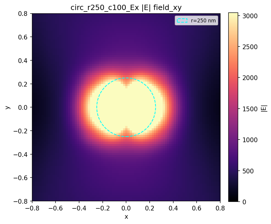
circ_r250_c100_Ex |E| x–y
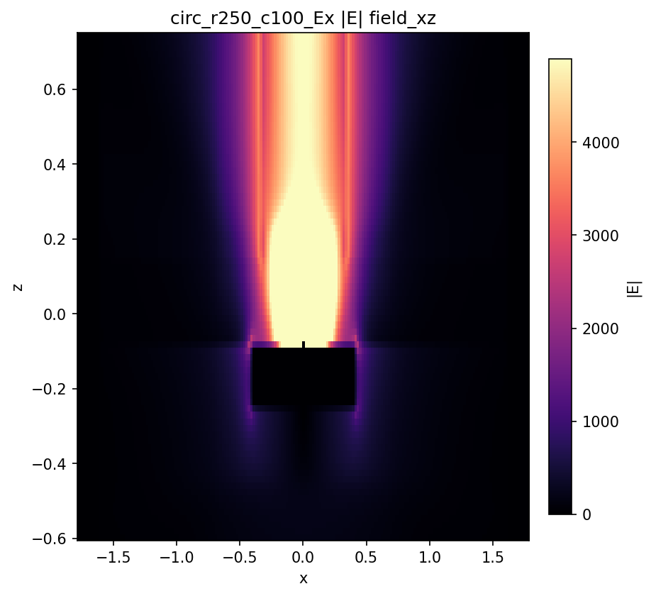
circ_r250_c100_Ex |E| x–z
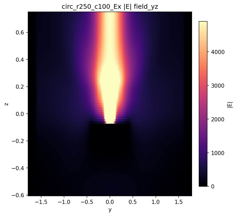
circ_r250_c100_Ex |E| y–z
TM — η = 74.21%
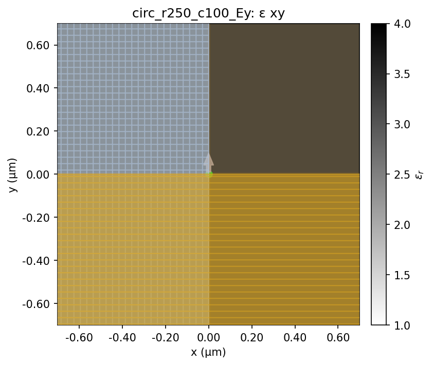
circ_r250_c100_Ey geometry x–y
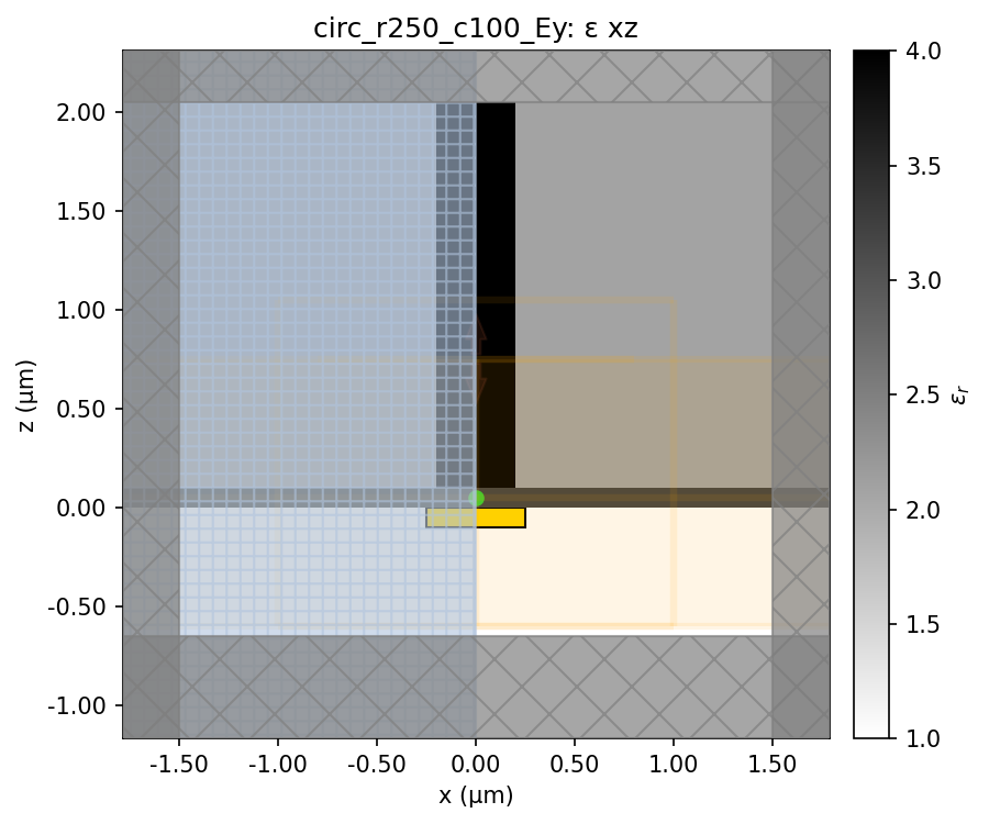
circ_r250_c100_Ey geometry x–z
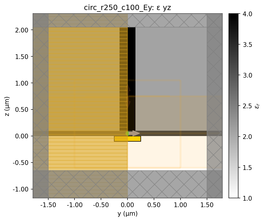
circ_r250_c100_Ey geometry y–z
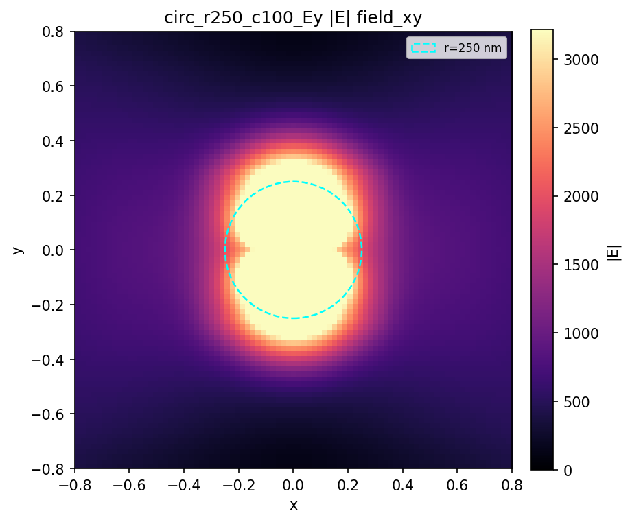
circ_r250_c100_Ey |E| x–y
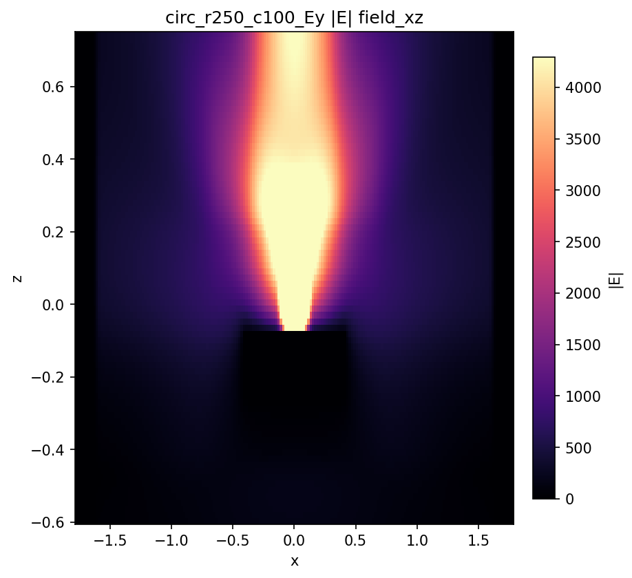
circ_r250_c100_Ey |E| x–z
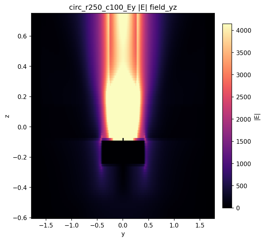
circ_r250_c100_Ey |E| y–z
Metrics: best_patch_c100_metrics.json
24 additional parametrized sweep reports exist under reports/ (excitation schemes, DBR variants, metal swaps, etc.).
Downloads
FDTD simulation study only -- no GDS/STL deliverable files exist in this tree.
Source: nanophotonic_devices/emitter_coupling/anthracene_coupling_chip_invdes_v2/