V1
This is the GDS used
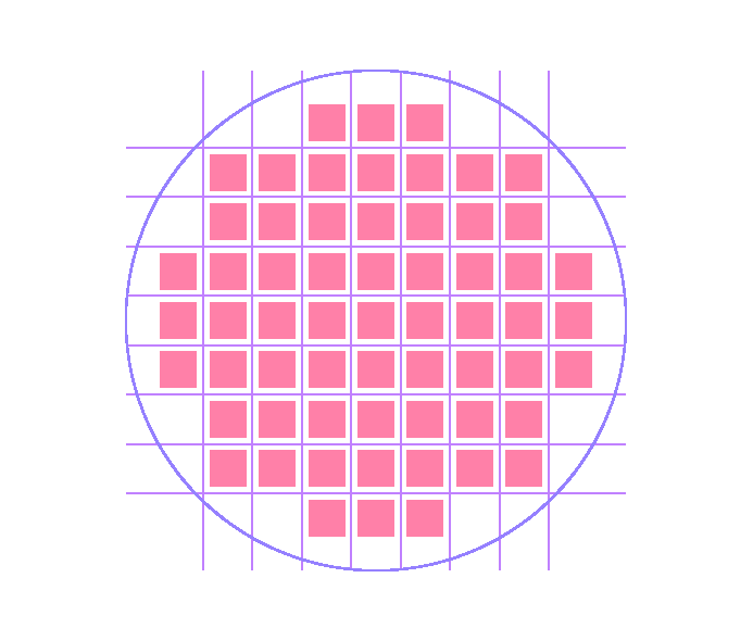
Just use layer 1 for now (dots, not dicing borders or wafer outline).
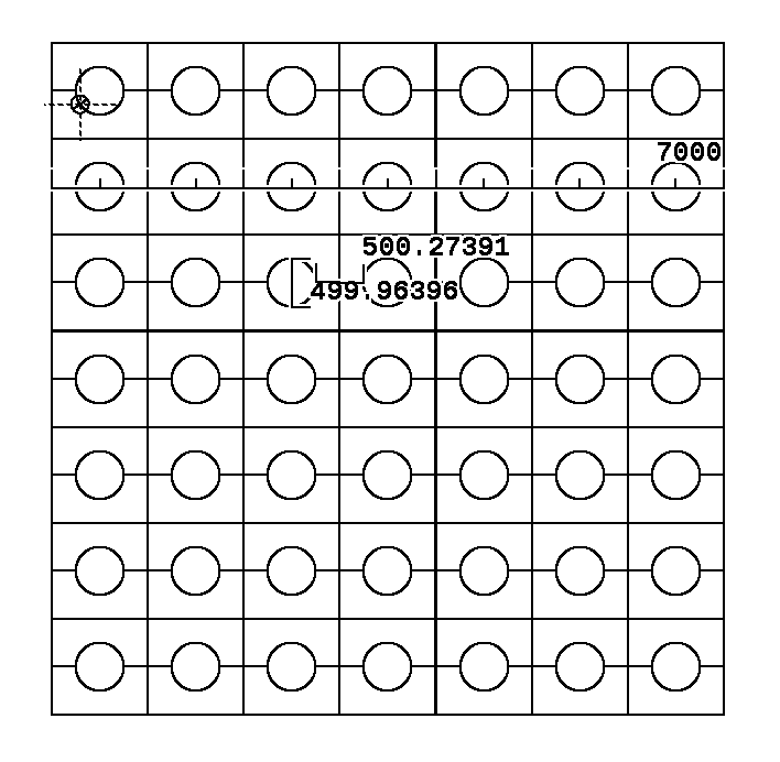
Each chip has a 7 mm pattern with 500 micron holes and 500 micron space between holes.
Spin coating
Exposure
Development
This is the GDS used
Just use layer 1 for now (dots, not dicing borders or wafer outline).
Each chip has a 7 mm pattern with 500 micron holes and 500 micron space between holes.
Spin coating
Exposure
Development