Jin et al 2022
jin2022micro-fabricated.pdf sm_jin2022micro-fabricated.pdf
Micro-fabricated mirrors with finesse exceeding one million
Jin et al 2022
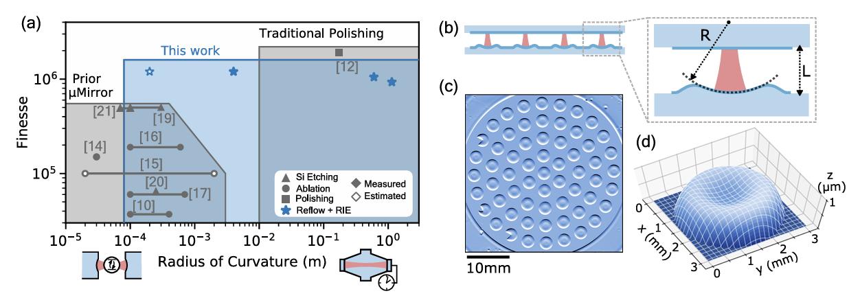
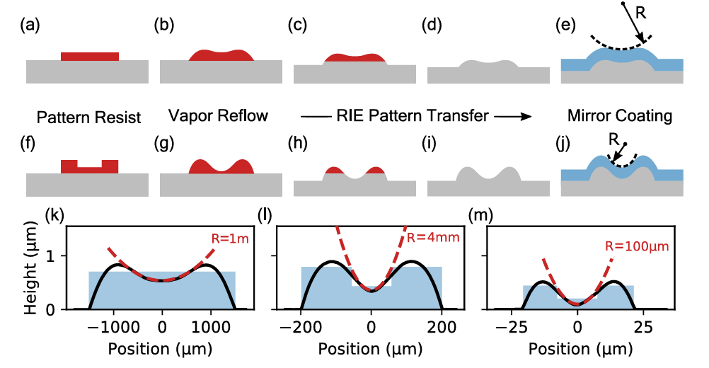
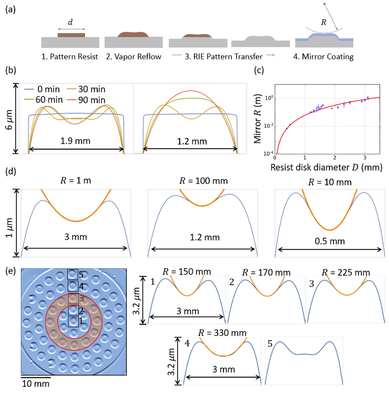
[!QUOTE] Through this fabrication approach, we use reflow techniques to create a resist profile that defines the shape of the mirror. Photoresist patterns (MICROPOSIT S1818, positive-tone) are first created on a super-polished substrate (e.g., fused silica) using UV lithography.
[!QUOTE] These resist patterns undergo reflow in a purpose-built solvent-vapor chamber containing propylene glycol methyl ether acetate (PGMEA), a standard solvent for the semiconductor industry; as the photoresist absorbs the solvent vapor, surface tension rounds any sharp corners as it seeks to minimize the surface area of the resist pattern
[!QUOTE] In the limit of complete reflow, this disk is transformed into a dome[31,32];how ever, for intermediate reflow times, a smooth parabolic surface is formed in the center of the resist pattern, as illustrated in Figs. 2(b)
[!QUOTE] Note that different etch rates for the photoresist and substrate result in a vertical rescaling of the pattern.
[!QUOTE] Weachieved control over the reflow by purposely elevating the temperature of the substrate a few degrees higher than the ambient temperature of the solvent vapor. Under this condition, the viscos ity of the photoresist can be tuned to permit a relatively fast reflow rate without worry of solvent vapor condensation. Compared with the traditional thermal reflow for making micrometer-scale lenses, this vapor-assisted approach proves to be efficient at mak ing larger structures on the scale of millimeters [30]. Particular attention must be paid to thermalization of the reflow chamber to ensure repeatability and uniformity of the reflow process. Further details and assessment of the fabrication process can be found in Supplement1SectionS2.
Supplementary information
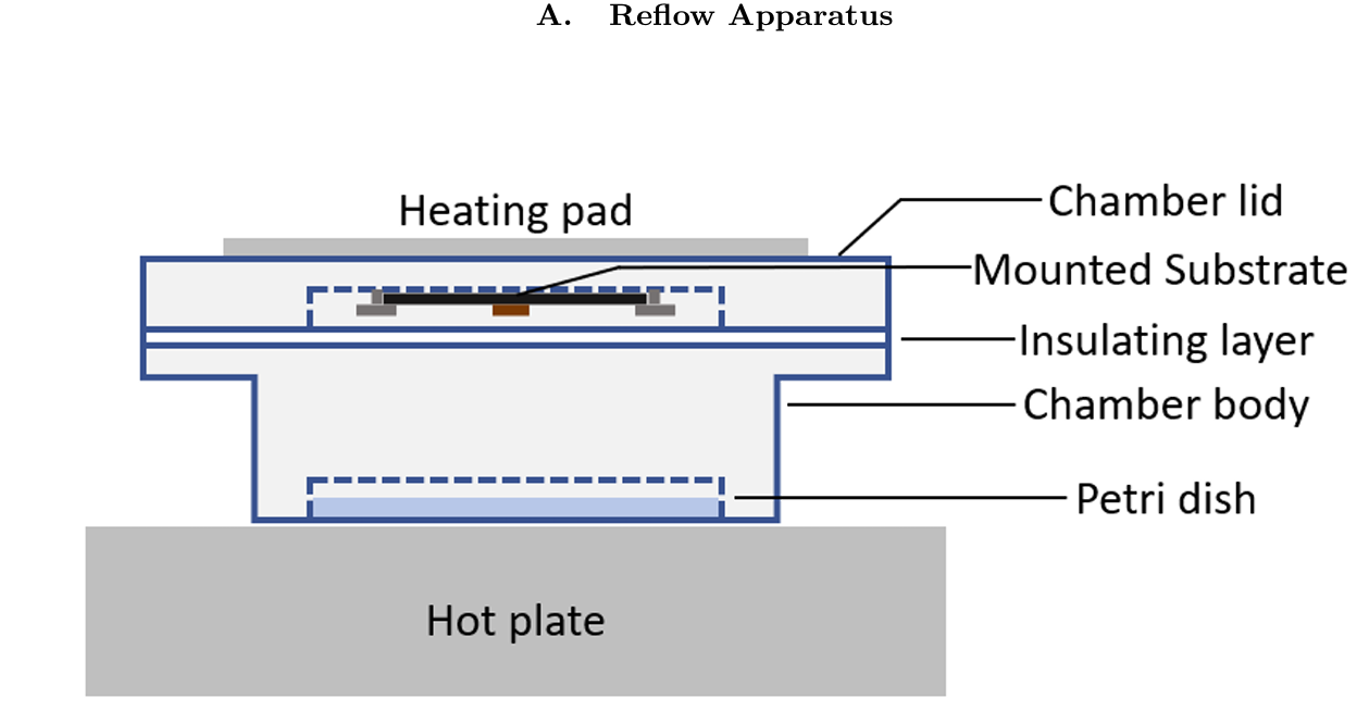
[!QUOTE] Because the desired shape of the reflowed photoresist is an intermediate state, precise control of the reflow is required to consistently obtain mirror surfaces with the desired R. To meet this requirement, we built a dedicated chamber to perform reflow under well-controlled vapor pressure and temperature. Fig. S1 shows a schematic of this apparatus. A petri dish filled with PGMEA is placed in the chamber to generate vapor, and a substrate with patterned photoresist is mounted on the chamber lid. An insulating layer between the body and lid allows us to maintain a temperature difference between the two parts. By using a hot plate underneath the chamber and a heating pad attached to the lid, we are able to independently control the temperature of the solvent vapor (and thus its vapor pressure) and the substrate. This control ensures a gradual reflow while preventing the solvent from dissolving the photoresist. Typical temperature settings for the solvent vapor and substrate would be approximately 45◦C and 50◦C, respectively. Under this condition, a 3 mm-diameter photoresist disk will reach a concave shape in approximately one hour. As long as we maintain adequate thermalization of this apparatus, we are able to consistently reproduce the same resist shape given identical initial disk diameters and reflow times.
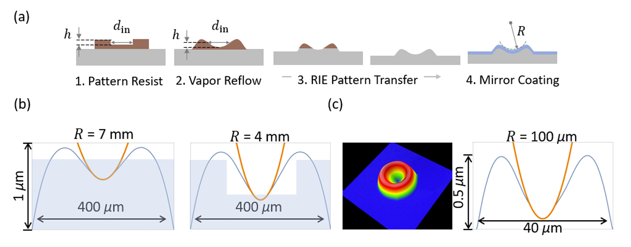
[!QUOTE] To achieve smooth transfer of the reflowed pattern, we develop an RIE recipe that preserves the surface quality of both the photoresist and substrates. Reactive ion etching of quartz/fused silica has been studied extensively. In particular, it has been shown in [S12, S13] that a plasma based on SF6 with a greater concentration of heavy noble gases (Ar or Xe) under low pressure can preserve ultrasmooth surfaces on quartz. At the same time, to avoid detrimental modification of the photoresist during etching (e.g. reticulation[S14]), we use low RF power and apply thermal grease to transfer heat between the substrate and carrier wafer. We carry out the etch using an Oxford 100 PlasmaLab, with pressure 4.5 mTorr, RF power 90 W, SF6 flow rate 4 sccm, Ar flow rate 14 sccm and helium backing on. This recipe typically gives a DC offset of 360 V with a 0.5 mm silica carrier wafer, S1818 resist etch rate of ∼100 nm/min and fused silica etch rate of ∼25 nm/min.