Saved in
G:\Shared drives\QLuster\product\nanophotonic_structures\anthracene_vertical_slot_coupler_v1\reports
session_report.html
Anthracene / Vertical Waveguide Coupling: Session Report
First major report covering everything simulated in this session: the baseline slot-waveguide design from the dry-run, a chain of ad hoc single-point and small-sweep variants exploring spacer thickness, crystal thickness, slot width, mirror type, and waveguide core material, culminating in the best design found so far. All coupling-efficiency numbers are at the emitter's 780 nm line unless noted otherwise. All simulations described here have actually been run on Tidy3D's cloud solver (not estimates).
Device concept
A 200 nm anthracene crystal (n=1.8) hosts a linear quantum-emitter dipole (780 nm) at its mid-plane. It sits on an optional SiO2 spacer, on top of a bottom boundary (a PEC mirror in most runs; also tested as a real DBR, and as no reflector at all). Directly above the crystal is a vertically-oriented waveguide -- either a Si3N4/TiO2 slot waveguide (two rails split by a narrow gap) or a solid rod, cladded in SiO2 -- propagating in +z. A dipole polarized across the waveguide's x-axis is the TE case; polarized along y is TM. Coupling efficiency is guided fundamental-mode power (mode monitor, +z) divided by total radiated power (flux box, all sides).
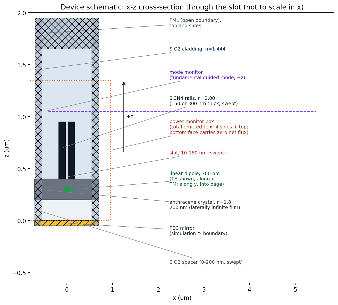
Device schematic (baseline slot-waveguide geometry)
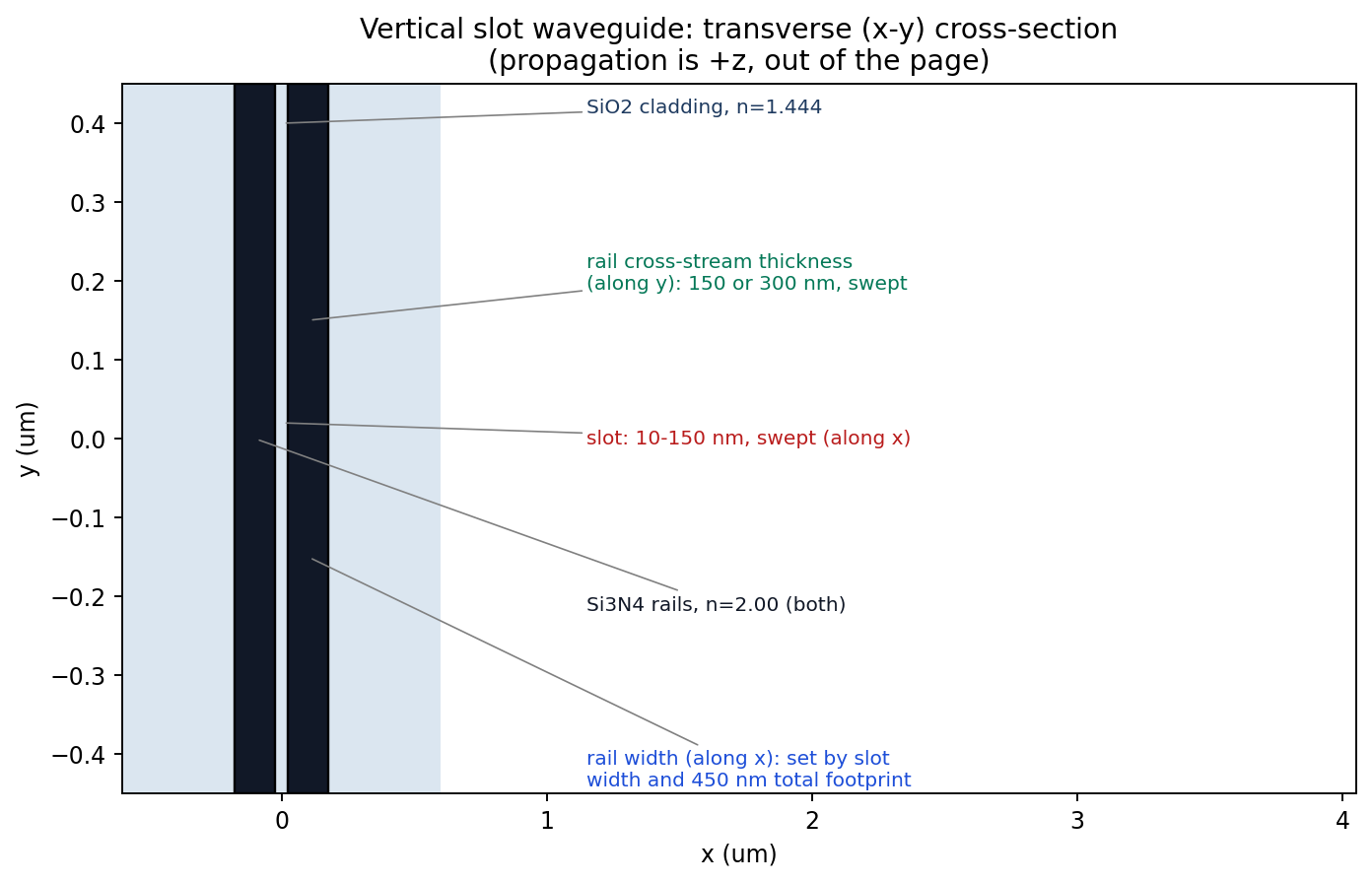
Vertical slot waveguide transverse cross-section
The whole session at a glance
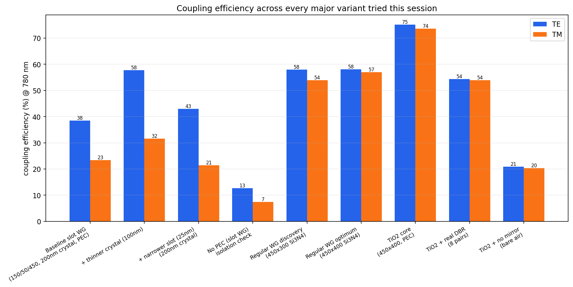
Coupling efficiency at every major milestone this session
Two findings dominate everything else: (1) a plain solid waveguide beats the slot design for this buried-emitter geometry, because the emitter sits below the whole footprint rather than inside the slot gap; and (2) core material index matters a lot -- swapping Si3N4 (n=2.0) for TiO2 (n=2.8) at the same dimensions took the best result from 58%/54% to 75%/74%. The PEC mirror is doing a lot of work too: replacing it with a real 8-pair DBR drops coupling by about a third, and removing the mirror entirely drops it by about two-thirds.
1. Baseline: slot waveguide
150 nm Si3N4 rails, 50 nm slot, 450 nm total footprint, 200 nm crystal, no spacer, ideal PEC mirror -- the nominal geometry from the original dry-run sweep design.
| Polarization | Coupling @ 780nm | Spectral range (750-850nm) |
|---|---|---|
| TE (dipole across slot) | 38.5% | 38.4-38.6% |
| TM (dipole along slot) | 23.4% | 19.2-32.1% |
TE is essentially flat across the band; TM rises steadily from 750 to 850 nm. This is the reference point for every comparison below.
2. SiO2 spacer sweep (0-200 nm)
Same geometry as the baseline, with a SiO2 layer of varying thickness inserted between the crystal and the PEC.
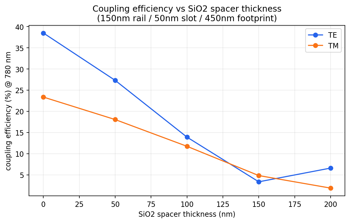
Coupling efficiency vs SiO2 spacer thickness
| Spacer (nm) | TE | TM |
|---|---|---|
| 0 | 38.5% | 23.4% |
| 50 | 27.3% | 18.1% |
| 100 | 13.9% | 11.7% |
| 150 | 3.4% | 4.8% |
| 200 | 6.6% | 1.9% |
Finding: 0 nm (crystal directly on the PEC) is optimal. Coupling falls monotonically to a minimum near 100-150 nm, consistent with the crystal moving out of the constructive-interference zone of the dipole's image in the mirror. The interference period (~270 nm half-wavelength in SiO2) suggests a second, weaker maximum may exist further out (~250-300 nm), untested here.
3. Crystal thickness (100 nm vs 200 nm)
Same slot geometry, no spacer, PEC -- crystal thickness reduced from 200 nm to 100 nm, halving the dipole's distance from both the PEC and the waveguide (50 nm each way instead of 100 nm).
| Crystal thickness | TE | TM |
|---|---|---|
| 200 nm (baseline) | 38.5% | 23.4% |
| 100 nm | 57.7% | 31.6% |
Finding: thinner is better. Roughly +19 points TE, +8 points TM -- moving the emitter closer to both the mirror and the waveguide's near field helps substantially.
4. Slot width (25 nm vs 50 nm)
200 nm crystal, no spacer, PEC, 150 nm rails, 450 nm footprint -- slot narrowed from 50 nm to 25 nm (rails widen correspondingly to keep the footprint fixed).
| Slot width | TE | TM |
|---|---|---|
| 50 nm (baseline) | 38.5% | 23.4% |
| 25 nm | 43.0% | 21.4% |
Finding: narrower slot helps TE (tighter mode confinement, better near-field overlap: +4.5 points) but slightly hurts TM (-2 points, since TM doesn't benefit from slot confinement and just sees wider rails).
5. Isolating the PEC's contribution (slot waveguide)
Same slot geometry (200 nm crystal, no spacer) with the PEC replaced by an open (PML) boundary and the domain extended below the crystal with SiO2, so downward-radiated power is lost instead of reflected.
| Configuration | TE | TM |
|---|---|---|
| With PEC (baseline) | 38.5% | 23.4% |
| No PEC (open boundary) | 12.6% | 7.5% |
Finding: the PEC accounts for roughly two-thirds of the coupling efficiency. Without it, ~20% of total power radiates straight down and is lost (verified via the flux monitor on that face), and the dipole's radiation-pattern asymmetry (weak along its own polarization axis) is clearly visible in the lateral-flux split.
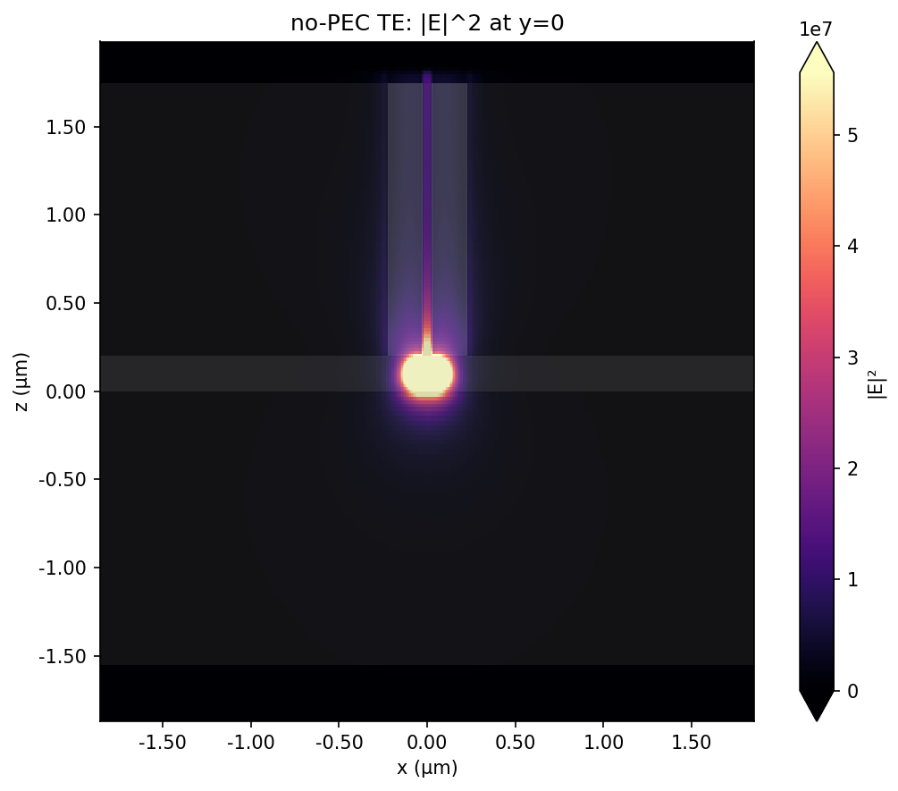
No-PEC field intensity: downward glow into the substrate that the PEC normally reflects back up
6. Discovery: a regular (non-slot) waveguide beats the slot design
Same crystal/spacer/PEC as the baseline, but the two-rail slot waveguide is replaced by a single solid Si3N4 rod (450 x 300 nm).
| Design | TE | TM |
|---|---|---|
| Slot waveguide (50 nm slot) | 38.5% | 23.4% |
| Regular (solid) waveguide | 58.0% | 53.9% |
Why: the emitter sits below the entire waveguide footprint, not inside the slot gap. A slot removes high-index material from directly above the strongest part of the dipole's near field; a solid rod keeps it there. The usual slot-waveguide advantage (field enhancement for emitters embedded in the gap) doesn't apply to this buried-emitter geometry.
A methodological note carried forward from here: each dipole polarization's simulation uses mirror symmetry (Ex: odd across x, even across y; Ey: the reverse), which restricts that job's own mode solve to one symmetry class -- so mode_index=0 is automatically the correct fundamental mode for that polarization, without needing the Ex/Ey energy-fraction classification the slot waveguide required.
7. Regular-waveguide dimension sweep (W x H)
Width (x, 300/450/600 nm) x thickness (y, 200/300/400 nm), Si3N4 core, otherwise the section-6 baseline.
TE coupling @ 780nm:
| W H | 200nm | 300nm | 400nm |
|---|---|---|---|
| 300 | 48.4% | 54.1% | 54.5% |
| 450 | 53.9% | 58.0% | 58.1% |
| 600 | 53.2% | 56.7% | 57.1% |
TM coupling @ 780nm:
| W H | 200nm | 300nm | 400nm |
|---|---|---|---|
| 300 | 43.4% | 54.1% | 57.5% |
| 450 | 45.3% | 53.9% | 57.0% |
| 600 | 43.4% | 51.1% | 53.8% |
Finding: TE peaks near W=450nm and saturates quickly with H; TM keeps climbing with H over this whole range and prefers narrower W. Best balanced point in the tested grid: W=450, H=400 nm (TE=58.1%, TM=57.0%). TM hadn't saturated at H=400nm, so a larger H may do even better.
8. Core material: TiO2 (n=2.8) instead of Si3N4 (n=2.0)
Best regular-waveguide geometry (450 x 400 nm), core material swapped to TiO2.
| Core material | TE | TM |
|---|---|---|
| Si3N4 (n=2.0) | 58.1% | 57.0% |
| TiO2 (n=2.8) | 75.1% | 73.6% |
Best result of the session. Both modes are broadband and essentially lossless in the mode solver (n_eff ~2.57/2.55, negligible imaginary part). Higher index contrast gives tighter confinement and better near-field overlap with the buried dipole.
Methodology fix along the way: the mode monitor's search bias (target_neff) was still set for the crystal index (1.8), appropriate for Si3N4 but not for TiO2's much higher n=2.8 -- the first attempt completely missed the true fundamental mode and gave spuriously low numbers (~2-8%). Corrected to target_neff=2.2 and rerun; verified against a free local mode solve before trusting the result.
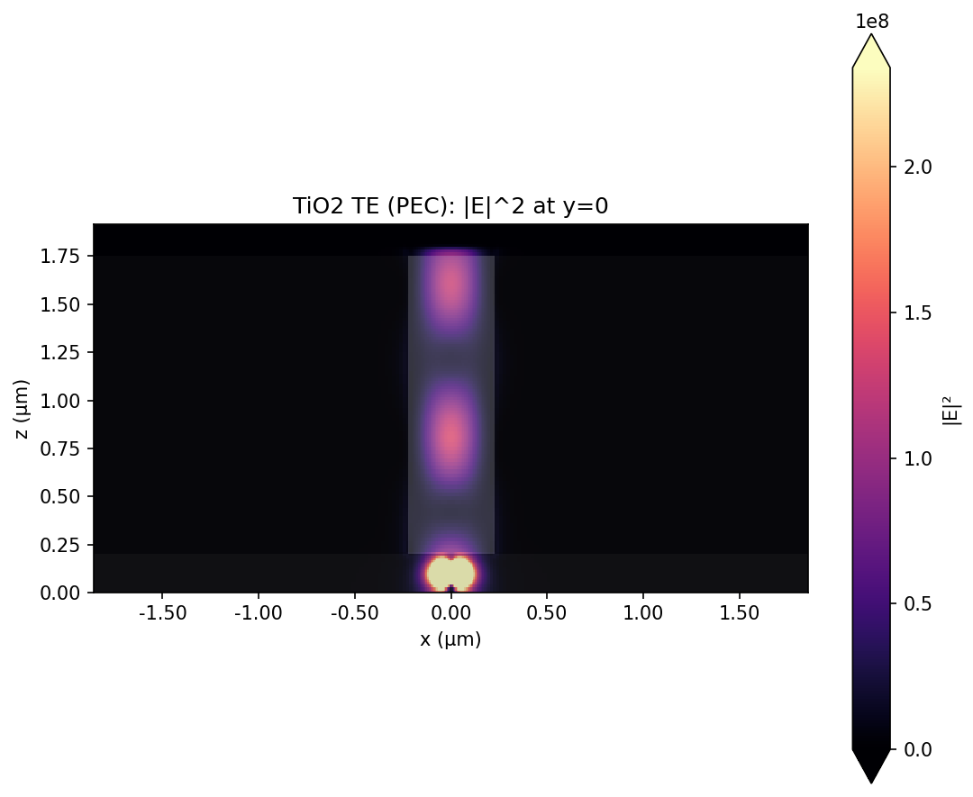
TiO2 TE mode field intensity: guided streak up the rod from the dipole
9. Real mirror: 8-pair TiO2/SiO2 DBR instead of ideal PEC
Best TiO2 geometry (450 x 400 nm), PEC replaced by a quarter-wave DBR (8 pairs, designed for 780 nm, ~1.64 um thick) on a SiO2 substrate terminated in PML.
| Mirror | TE | TM |
|---|---|---|
| Ideal PEC | 75.1% | 73.6% |
| 8-pair DBR | 54.3% | 54.0% |
Finding: the DBR reflects almost perfectly (downward flux ~0%, matching the PEC) but coupling is still notably lower. The gap isn't about reflected power -- it's about angle and phase: a PEC reflects every angle with the same simple phase shift, while a quarter-wave DBR's reflection phase and magnitude vary with incidence angle. The dipole's near field contains many angular components, and only the near-normal ones see the DBR's designed response, so the constructive interference that boosts coupling with a PEC is only partially reproduced.
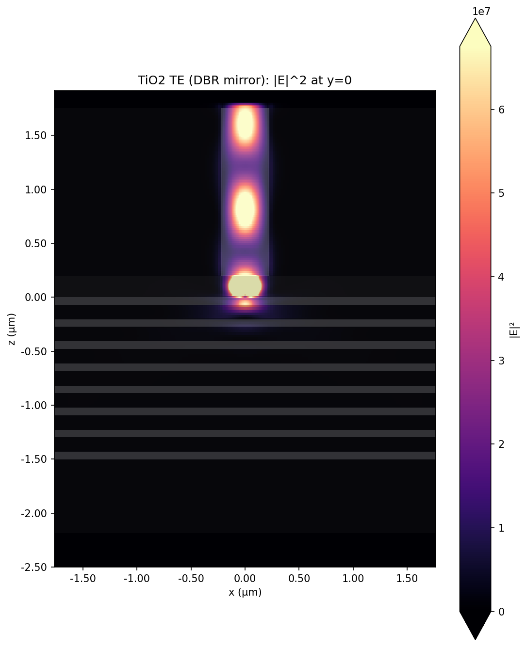
DBR field intensity: layer stack visible below the crystal, negligible field penetrates it
10. No mirror at all: bare crystal/air interface
Same TiO2 waveguide, PEC/DBR removed entirely -- just air (n=1) below the crystal, terminated in PML. Isolates plain Fresnel/total-internal reflection at the n=1.8/n=1 step (critical angle ~33.75 deg) with no engineered mirror.
| Bottom boundary | TE | TM | Downward loss |
|---|---|---|---|
| Ideal PEC | 75.1% | 73.6% | 0% |
| 8-pair DBR | 54.3% | 54.0% | ~0% |
| Bare air (no mirror) | 20.9% | 20.3% | ~14.5% |
Finding: bare index contrast alone recovers a real but partial fraction of the benefit -- about a third of what the DBR provides, about a quarter of the ideal PEC. An engineered reflector is doing substantial, necessary work; it isn't just "any index step would do."
Cost accounting
40 billed simulations run this session; total real cost: 1.011 FlexCredits. All jobs were validated and cost-estimated (via Tidy3D's non-billed estimate_cost) before submission, per the project's FlexCredit guardrail.
Mid-session, we noticed the pre-run cost estimate was running 4-10x higher than the real (post-run) billed cost, because the configured run_time (3 ps) was oversized relative to how fast the fields actually decay -- solver logs showed the automatic shutoff triggering within the first 1-2% of allotted time steps across every geometry tested (slot, regular, TiO2, DBR, no-PEC alike). run_time was halved to 1.5 ps, bringing typical-size jobs to within about 2x of their real cost (matching the real-cost floor observed for smaller jobs, ~0.025 FC/job) while retaining a 35-50x safety margin over the observed decay times. This is now the default for all runs going forward.
Summary comparison table
| Configuration | TE @ 780nm | TM @ 780nm |
|---|---|---|
| Baseline slot WG (150/50/450, 200nm crystal, PEC) | 38.5% | 23.4% |
| + thinner crystal (100nm) | 57.7% | 31.6% |
| + narrower slot (25nm) (200nm crystal) | 43.0% | 21.4% |
| No PEC (slot WG) isolation check | 12.6% | 7.5% |
| Regular WG discovery (450x300 Si3N4) | 58.0% | 53.9% |
| Regular WG optimum (450x400 Si3N4) | 58.1% | 57.0% |
| TiO2 core (450x400, PEC) | 75.1% | 73.6% |
| TiO2 + real DBR (8 pairs) | 54.3% | 54.0% |
| TiO2 + no mirror (bare air) | 20.9% | 20.3% |
Conclusions and open directions
- Best design found so far: solid (non-slot) TiO2 waveguide, 450x400 nm, 200 nm crystal, no spacer, ideal PEC -- TE=75.1%, TM=73.6%.
- Every geometric lever tried (thinner crystal, no spacer, solid vs. slot, higher-index core) helped in the same direction: get more high-index material as close to the dipole as possible.
- The PEC mirror is not a detail -- it is the single largest lever in the whole study. A real DBR captures roughly 70% of its benefit; no mirror at all captures roughly 25-28%.
- Not yet tried: combining the biggest wins together (TiO2 core + 100nm crystal + no spacer + optimized W/H), a W x H sweep at n=2.8, spacer values beyond 200nm to find the next constructive-interference peak, and DBR pair-count/design-wavelength tuning.
- The
run_timereduction and TE/TM symmetry-based mode selection (both discovered mid-session) should carry forward into any future full-sweep run of this project.