Facing curved-mirror atom cavity#
This page is a geometry-review checkpoint for the next atom-to-waveguide
campaign. It compares the saved intermediate structures using only
geometry–metric pairs with matching fingerprints, then shows a compact
single-etch parameterization of the recurring ((( ))) mirror family.
Important
The four clean drawings below are parameterized geometries, not claimed simulation results. Their purpose is to verify the physical interpretation before a large GPU sweep. Cyan is the literal vacuum-access gap, blue-gray is silica, gold is silicon, and the red star is the atom.
What the intermediate designs actually show#
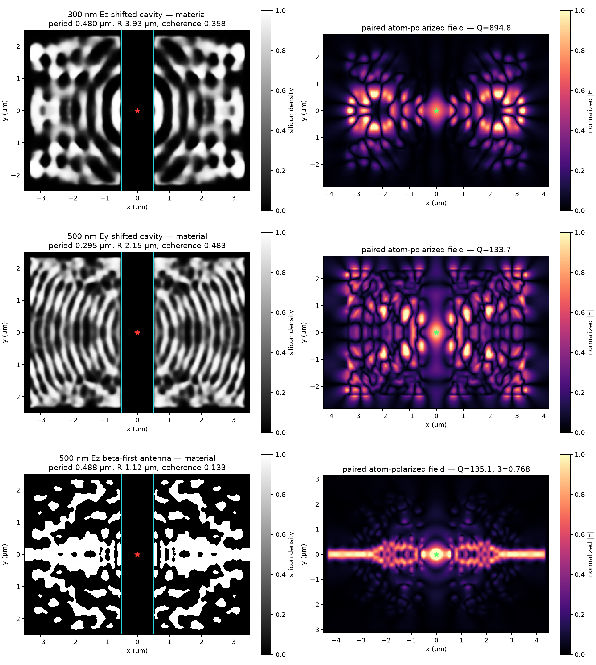
Every field is paired to the material array saved with that field. The cyan lines mark the 1 µm gap. The parabolic fit searches both correlation length and radius; neither is supplied in advance.#
The comparison supports the curved-mirror hypothesis, with important qualifications:
Recoverable paired structure |
Relevant result |
fitted period |
fitted radius |
parabolic coherence |
|---|---|---|---|---|
300 nm Ez shifted cavity, iteration 84 |
dense Q 894.8; ringdown Purcell 7.42 |
0.480 µm |
3.93 µm |
0.358 |
500 nm Ey shifted cavity, iteration 35 |
dense Q 133.7; ringdown Purcell 3.10 |
0.295 µm |
2.15 µm |
0.483 |
500 nm Ez beta-first antenna, update 60 |
Q 135.1; total β 0.768 |
0.488 µm |
1.12 µm |
0.133 |
The 300 nm Ez campaign reached an even better independent audit at Q 1653 and ringdown Purcell 13.18, although that best audit did not retain a separately paired field snapshot. Its retained iteration-84 geometry still clearly shows nested fronts around the gap. The independently initialized 500 nm Ey branch formed a cleaner curved grating with the strongest fitted spatial coherence. The beta-first branch instead formed an irregular waveguide antenna: it coupled well, but its weak spatial coherence and dirty, detuned pole distinguish it from the cavity-forming branches.
This is evidence of a useful architectural prior, not proof that curvature alone causes high Q. Thickness, polarization, objective, and binarization also differ among the campaigns.
Why the earlier headline numbers are not all seeds#
The no-gap optimized nanobeam reached validated Q 187,133, but it does not solve free-space atom access.
The adiabatic-gap branch reported transient Q above 10,000 while dielectric still occupied most of the future gap. After the gap became literal its recoverable Q remained below about 750 and the atom overlap was weak.
The original scratch branch reached Q 199 and Purcell 18, but used genuinely 3-D voxel controls. It is excluded because it cannot be fabricated by a single etch.
The 150 nm extruded branch saturated near LDOS 1.405 and Q 25.1. It is useful negative evidence for weak vertical confinement, not a geometry seed.
Proposed parameterization#
Each mirror front is a parabola in the lithographic plane,
[ |x| = x_n - \frac{y^2}{2R_n}, ]
and has a finite material width. The inner and outer period, duty cycle, curvature radius, and transverse aperture are joined by a smooth apodization. The full design variables are:
slab thickness and exterior cladding index;
mirror count and the first-front offset from the gap;
inner/outer period and silicon duty cycle;
inner/outer curvature radius and aperture;
apodization exponent, material polarity, and terminal waveguide width.
The air gap is not part of the parameterization. It is imposed after geometry
construction, so even an extreme curvature cannot place silicon or silica in
-0.5 < x < +0.5 µm. The generated 2-D mask is uniformly extruded through the
chosen slab thickness.
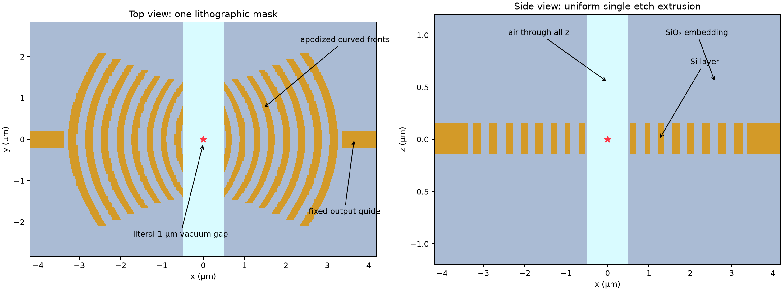
The oxide interpretation is literal: outside the gap, Si ribs are surrounded above, below, and laterally by SiO₂. The complete gap is air through z.#
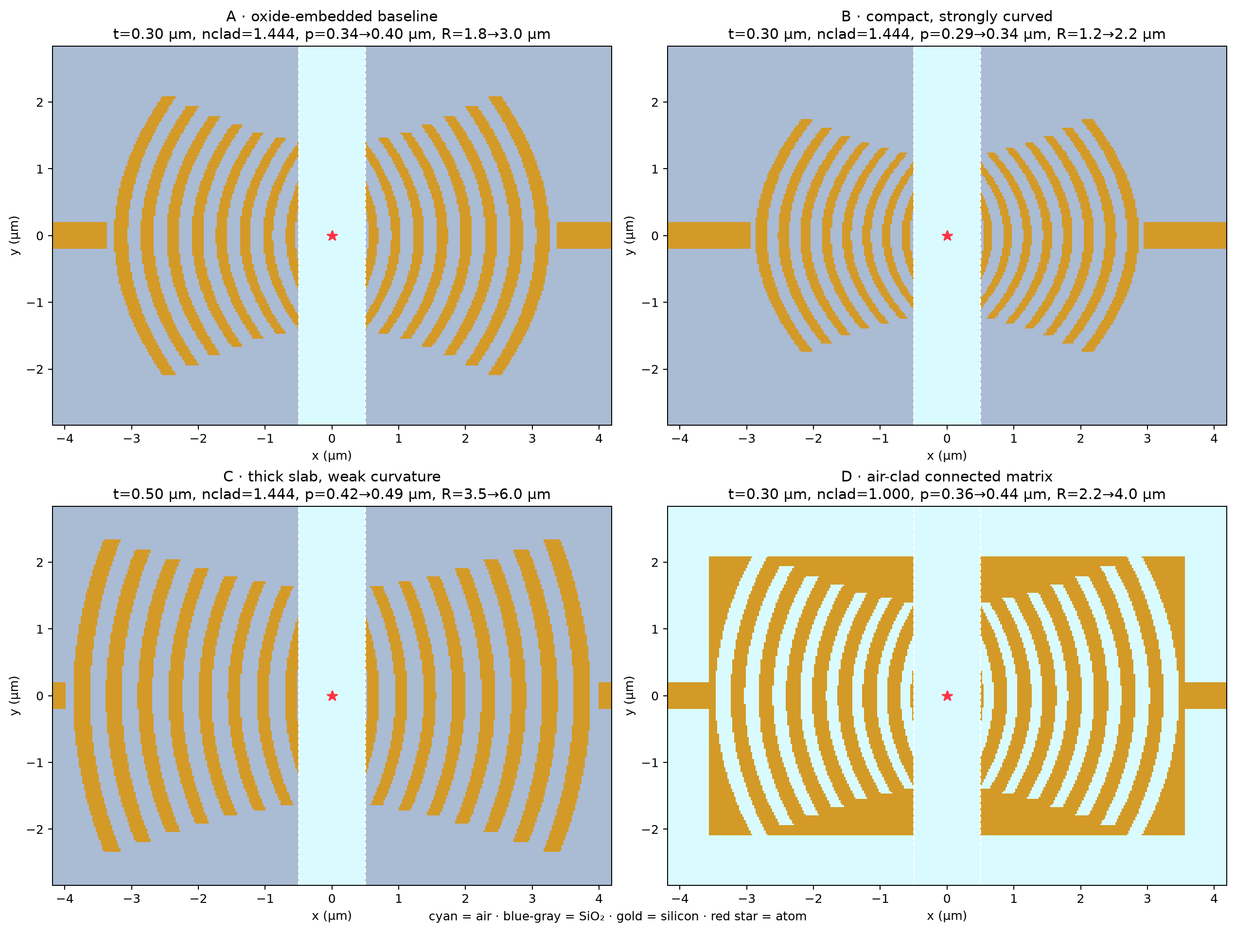
A is the recommended oxide-embedded baseline. B explores stronger focusing, C tests a thick weakly curved device, and D preserves an air-clad fabrication option by etching curved trenches into a connected silicon matrix.#
The exact parameters and paired evidence fingerprints are available as
curved_mirror_study.json.
Why sweep silica embedding#
Silica embedding is a plausible way to reduce diffraction across the 1 µm air gap: lowering the Si/background index contrast expands the transverse mode in the exterior region before it reaches the abrupt air opening. It is not unconditionally better. The same reduced contrast weakens each Bragg front, so an oxide design may need more periods or a longer mirror to recover its intrinsic Q. The sweep will therefore compare air and silica at equal physical aperture and will enlarge the mirror only when the measured attenuation per period requires it.
Sweep acceptance order#
The GPU sweep will be hierarchical rather than a blind Cartesian product:
screen thickness, cladding, period, and duty cycle with short broadband FDTD and reject candidates without a clean atom-coupled stop-band pole;
sweep curvature, aperture, first-front offset, and apodization on the viable cross-sections;
lengthen only the leading mirrors and measure whether Q rises exponentially with mirror count;
independently replay the leaders for Q, atom LDOS/Purcell, radiation loss by face, and guided-mode β;
hand only a literal binary, minimum-feature-compliant leader to shifted guided-Purcell optimization.
Short screens rank clean atom-frequency pole evidence without paying for a mode solve on every weak geometry. The long finalist audits rank guided Purcell and report β; they will not rank β alone, because high branching ratio with negligible total emission is not the desired atom interface.
The exact active grid, all 690 nominal variations, literal current geometry, LDOS spectra, and eventual finalist fields are shown on the live sweep dashboard.