
Ez-bandgap quasi-2D atom interface#
Fabrication stop — the suspended-pillar topology is rejected
The calculations below establish useful \(E_z\) bandgap and surface-mode physics, but the simulated SiN regions are disconnected pillars in air. They are not a fabricable suspended membrane and will not be used as the seed for the atom interface. The Q, wavelength, and field metrics remain numerical reference evidence, not a device claim.
Why the previous run was stopped#
The paused atom-to-waveguide optimizer reached 26.4% best beta, but 98.2% of its remaining unguided radiation escaped through the \(\pm z\) faces. Its \(E_y\) dipole pattern and the Zhang-style TE-like seed were fundamentally mismatched to the desired atom interface. Rotating only the dipole would not fix that: the original triangular air-hole slab has \(E_x/E_z=0\) by parity for its fundamental edge mode.
This campaign reverses the order of work:
prove that a unit cell excludes in-plane \(E_z\) propagation;
build a finite-height edge from that lattice;
find a stable \(E_z\) surface pole;
localize that surface pole in both in-plane directions;
only then optimize LDOS, Q, and waveguide beta.
1. Unit-cell bandgap screen#
FDTDX now includes a raster-based plane-wave eigensolver for the scalar 2D \(E_z\) problem. It accepts arbitrary primitive-cell permittivity, so the screen is not restricted to analytic circles.
import fdtdx

k, ticks, labels, lattice = fdtdx.high_symmetry_path(
    "triangular", points_per_segment=24
)
epsilon = fdtdx.periodic_circle_cell(
    lattice_vectors=lattice,
    radius=0.24,                 # r/a
    epsilon_background=1.0,
    epsilon_circle=2.05**2,      # Si3N4 post
    grid_shape=(256, 256),
)
bands = fdtdx.solve_ez_bands(
    epsilon,
    lattice_vectors=lattice,
    k_points=k,
    plane_wave_order=7,
    num_bands=6,
)
first_gap = next(g for g in bands.gaps() if g.lower_band == 1)
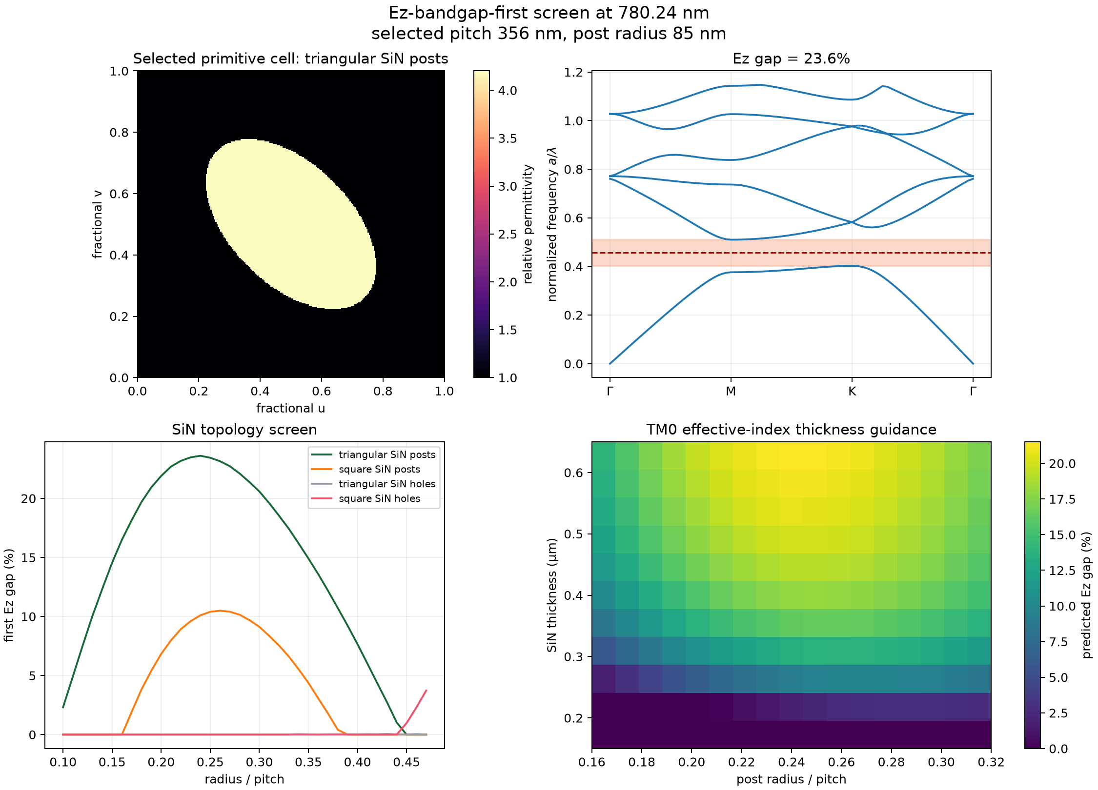
The triangular SiN-post lattice has a converged 23.56% first \(E_z\) gap from \(a/\lambda=0.40252\) to 0.51002. At 780.24 nm, the infinite-height mapping gives \(a=356.0\) nm and \(r=85.4\) nm. Air holes in SiN do not show a useful first \(E_z\) gap; this is why reusing the earlier hole slab was the wrong topology.#
The thickness panel is an effective-index screen, not a 3D result. It predicts no gap for a 150 nm SiN film, 3.0% at 200 nm, 13.9% at 300 nm, 18.1% at 400 nm, and 20.1% at 500 nm. The finite 3D sweep therefore began at 300–500 nm instead of silently assuming the old 150 nm film.
2. Fabrication audit and replacement topologies#
The original screen optimized optical contrast without enforcing material connectivity. That was a geometry-definition error. A follow-up converged PWE screen compared the two practical replacements and a connected single-etch variant:
topology at 780.24 nm |
converged first Ez gap |
fabrication assessment |
|---|---|---|
disconnected SiN pillars in air |
23.56% |
rejected: unsupported islands |
SiN pillars embedded in SiO\(_2\), \(r/a=0.29\) |
3.93% |
fabricable, but optically marginal; \(a=284\) nm and \(r=82\) nm |
circular air holes in a continuous SiN slab |
no useful gap |
fabricable, but wrong topology for the required Ez polarization |
connected SiN nodes and ribs, etched air voids |
10.62% at 30 nm ribs; 6.92% at 40 nm; 3.72% at 50 nm |
single connected mask; finite-height validation still required |
The connected-network row is not a disguised pillar process. Every SiN node is joined to its six neighbors, so the complement is an array of rounded triangular air holes etched through one continuous film. The quoted gaps are infinite-height 2D screening results. A 300 nm air-clad slab has only about \(n_\mathrm{eff}=1.70\) for its symmetric TM0 mode, reducing the corresponding screened gaps to approximately 6.1%, 2.8%, and 0.7%. At 500 nm thickness the effective index rises to about 1.92 and gives more margin. Full 3D FDTD, a minimum-feature audit, and the 500 nm atom-clearance notch remain mandatory.
3. Rejected finite-pillar reference#
This archived numerical reference is an array of disconnected vertical SiN posts. Its in-plane mask is extruded uniformly through one film thickness, so it was quasi-2D rather than free-voxel 3D, but extrusion alone does not make the isolated regions mechanically realizable. A z-oriented atom sits 500 nm from the nearest post surface.
from benchmarks.cases.ez_bandgap_quasi2d_cavity.geometry import (
    EzEdgeCavityParameters,
    rasterize_ez_edge_cavity,
)

params = EzEdgeCavityParameters(
    slab_thickness_um=0.400,
    lattice_constant_um=0.37181,
    post_radius_um=0.09295,
    atom_clearance_um=0.500,
    edge_retreat_um=0.120,
    taper_periods=4.0,
    tapered_row_count=1,
    central_radius_scale=0.80,
)
geometry = rasterize_ez_edge_cavity(params)
Every rasterization checks the literal circle-to-atom distance. Tests also require exact \(x\) symmetry and confirm that changing the central post radius moves its center so the 500 nm surface clearance remains fixed.
4. Full 3D GPU-FDTD result for the rejected reference#
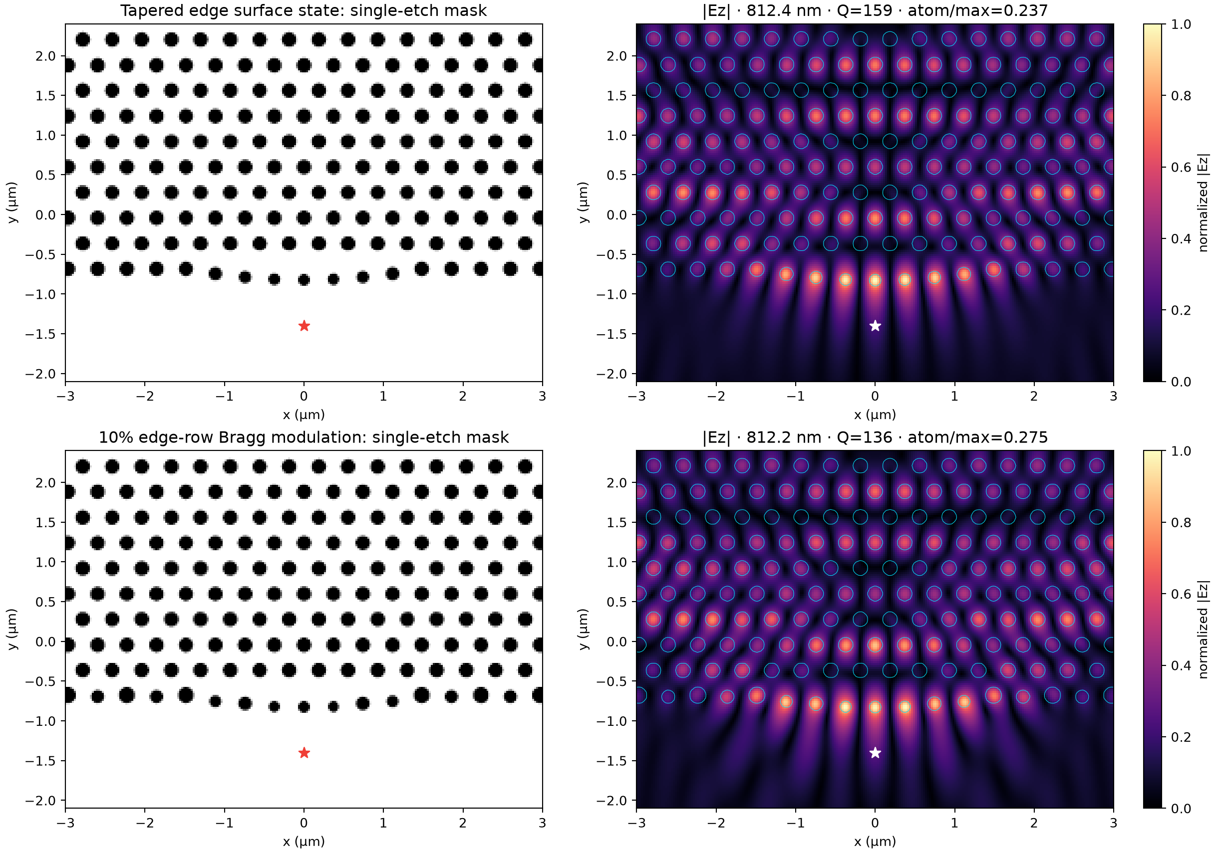
Top: the strongest unmodulated edge state. Its 812.43 nm pole has Q=159.2, \(|E_z|_\mathrm{atom}/\max|E_z|=0.237\), and peak \(|E_z|\) is 24.0× the larger of peak \(|E_x|\) and \(|E_y|\). Bottom: a 10% alternating-radius modulation improves atom/peak overlap to 0.275, but does not reduce the measured edge \(x_\mathrm{RMS}\) extent (1.52 µm versus 1.50 µm). It therefore remains a surface band, not a compact quasi-2D cavity.#
The favorable result is polarization: the mode is genuinely \(E_z\)-dominated and its field reaches the atom-facing air region. The unfavorable result is localization: a point dipole launches the state along much of the front row. The modest Bragg modulation moves field toward the atom but does not open a strong enough surface stopband.
5. Parameter sweeps#
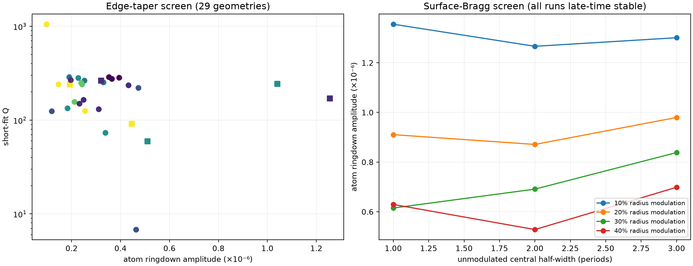
Left: 29 edge geometries spanning retreat, taper length, tapered-row count, and central-radius scale. Squares change the central radius; circles retain the bulk radius. Right: 12 surface-Bragg geometries spanning 10–40% alternating-radius modulation and one to three unmodulated central periods. The plotted Q values are short-screen fits; final numbers come only from the 2.5 ps audits above.#
The strongest atom ringdown came from reducing the central front-row radii to 80% while preserving surface clearance. Larger edge retreat can increase apparent short-window Q, but long audits show that it also moves field back into the crystal. The first Bragg attempt did not shrink the lateral mode and is recorded as a negative result rather than presented as a cavity.
6. PML stability hardening#
The first full-array runs grew exponentially after the source turned off. This was not a high-Q mode: harmonic inversion found no positive-Q pole and fields reached \(10^{32}\). Two solver-side safeguards were required:
fdtdx.extend_material_to_pml(...)continues the last physical material cross-section through the absorber instead of rasterizing more post periods inside CPML;fdtdx.auto_boundary_config(..., stabilize_evanescent=True)sets a wavelength-aware complex-frequency shift. This cavity required \(\alpha=0.2\,\omega\epsilon_0\); 0.05 still left a slow growing mode.
boundary_config = fdtdx.auto_boundary_config(
    pml_layers=12,
    wavelength=780.24e-9,
    stabilize_evanescent=True,
)
boundaries, constraints = fdtdx.boundary_objects_from_config(
    boundary_config, volume
)

# After the parameterized geometry is applied:
arrays = fdtdx.extend_material_to_pml(objects, arrays)
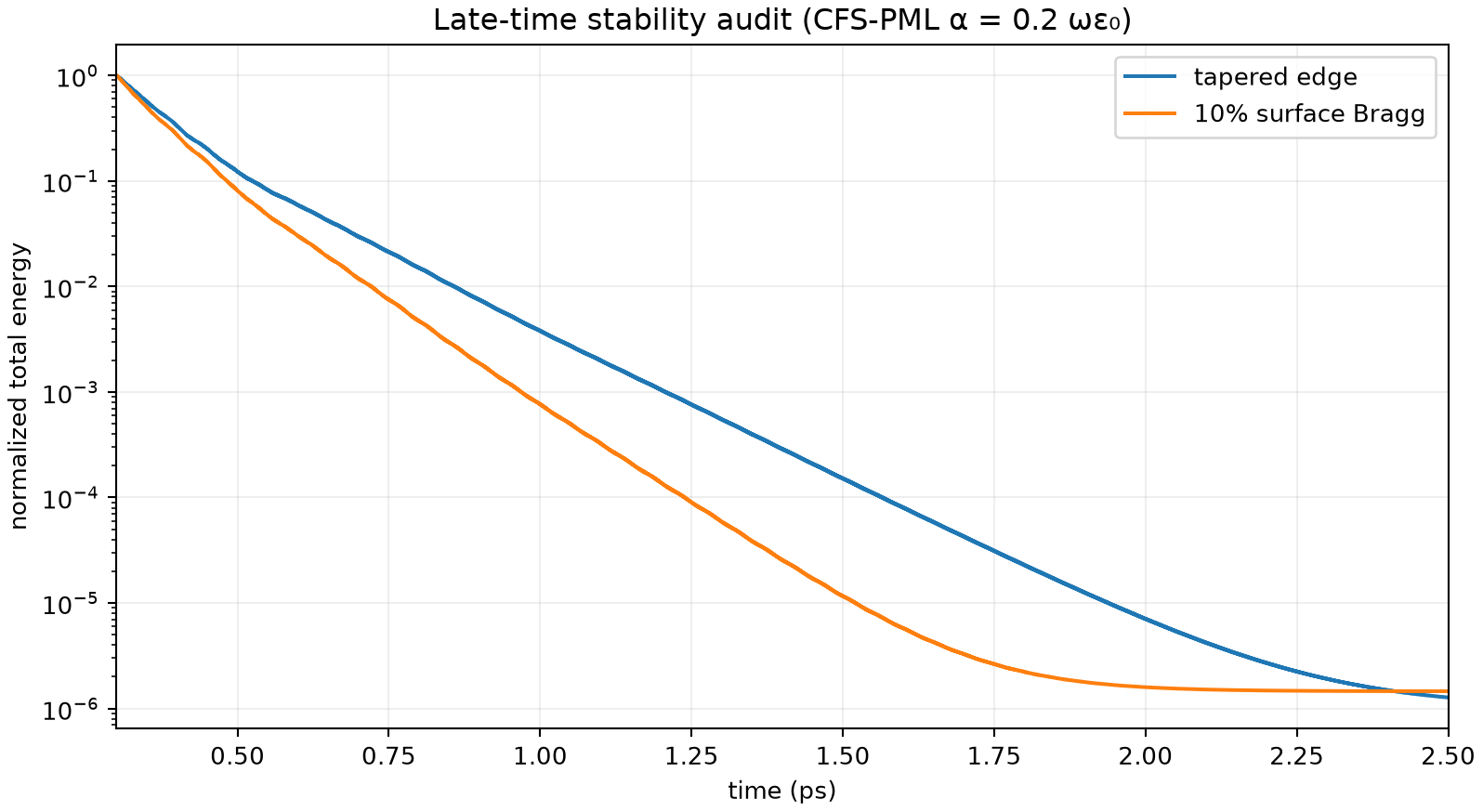
Both displayed field solutions pass the fail-closed late-time gate: total energy decays rather than merely remaining finite. A growing trace is excluded before Q fitting.#
Current conclusion and next experiment#
The disconnected-pillar branch is stopped. It demonstrated that a rod-like dielectric topology supplies the desired \(E_z\) physics, but it is not a candidate device. Ordinary circular holes do not reproduce that gap.
The leading replacement is the connected SiN node-and-rib network in a thicker air-clad membrane. Oxide-embedded pillars are the fallback if the connected network loses its gap in full 3D. The next sweep must:
use a literal connected-material constraint and a declared minimum rib width;
sweep 300, 400, and 500 nm film thickness before building an edge defect;
verify the bulk gap and radiation continuum in full 3D rather than relying on effective index;
preserve a true 500 nm air-clearance corridor for the atom;
compute the surface-band dispersion, rather than guessing a real-space modulation period;
place a defect inside a verified 1D surface stopband (position dimerization is the leading option);
field-audit lateral localization before starting LDOS or inverse-design optimization.
That sequence prevents another optimizer from spending a day improving an extended or numerically unstable state.