
Optimization campaign atlas#
Every FDTDX cavity and atom-interface optimization in one visual directory. Cards pair the actual optimized geometry with its simulated field, so related experiments remain distinguishable even when their internal campaign names are similar. Live pages continue to refresh; frozen, paused, and stopped pages preserve the last trustworthy checkpoint and the reason the campaign ended.
8.4 µm silicon nanobeam · adaptive waveform frontier
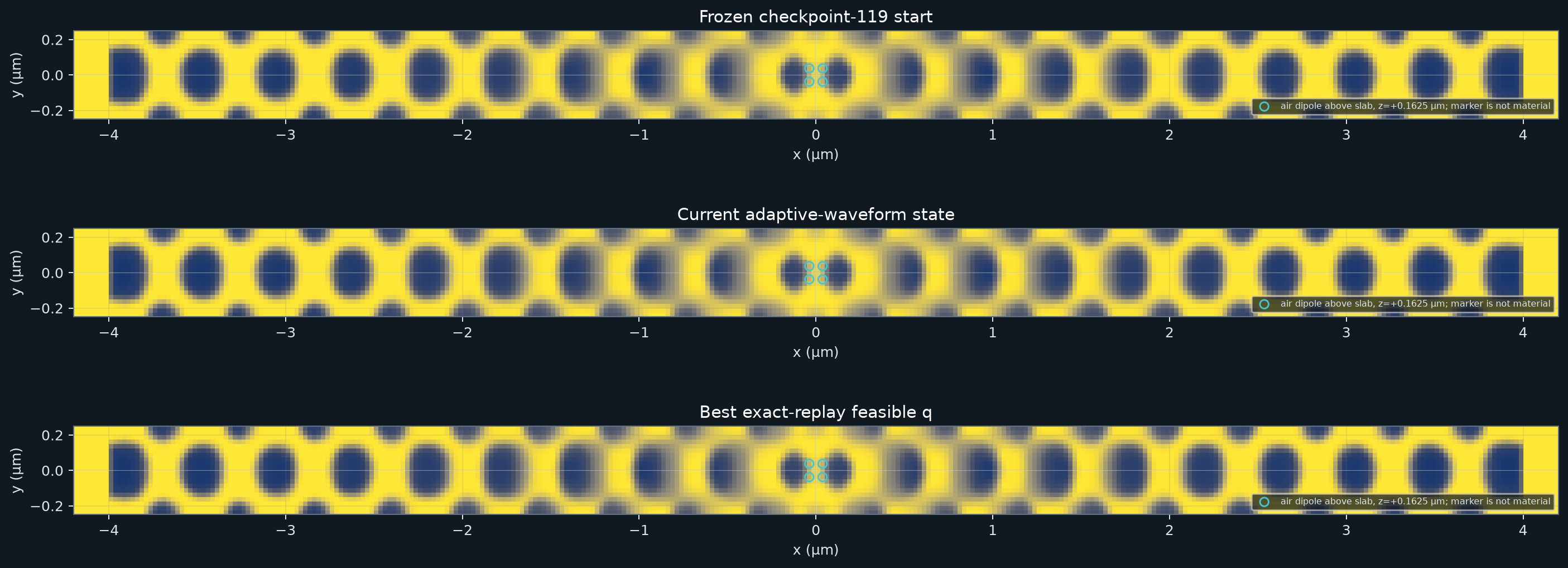
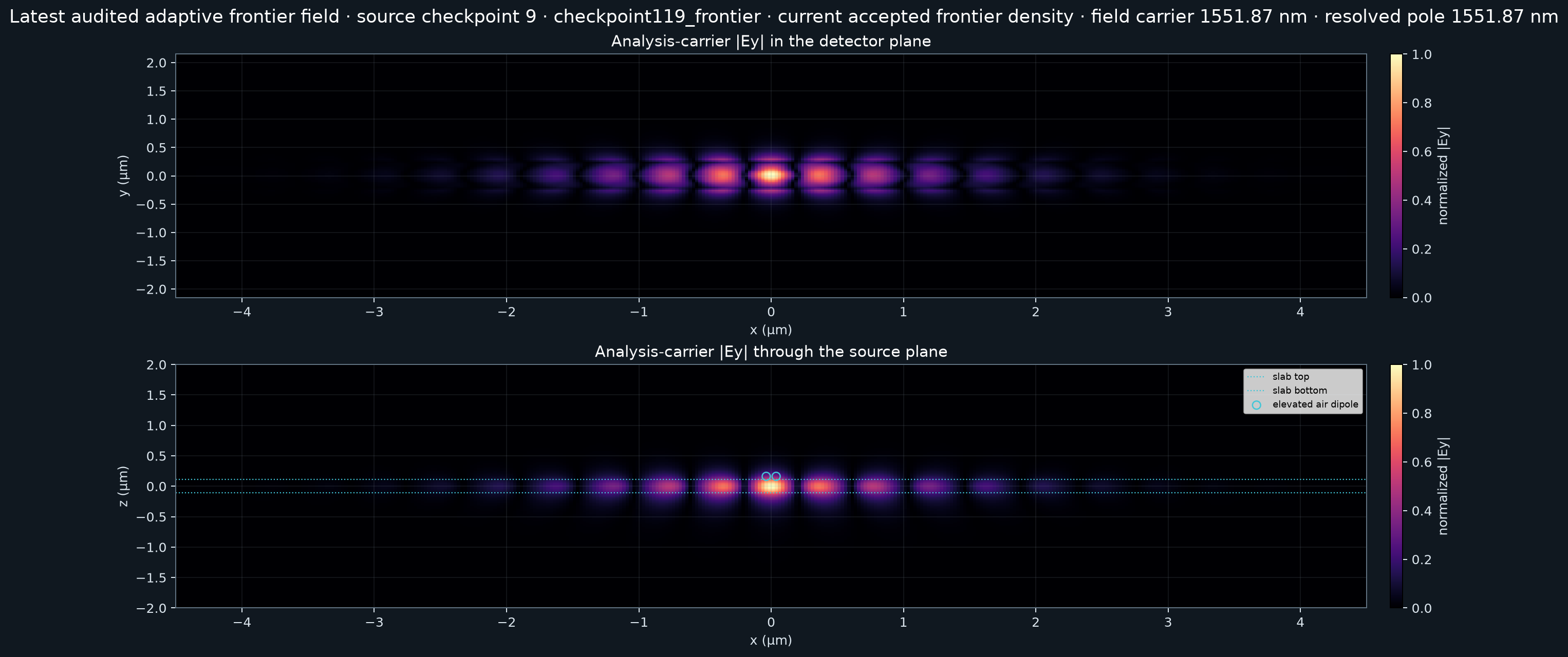
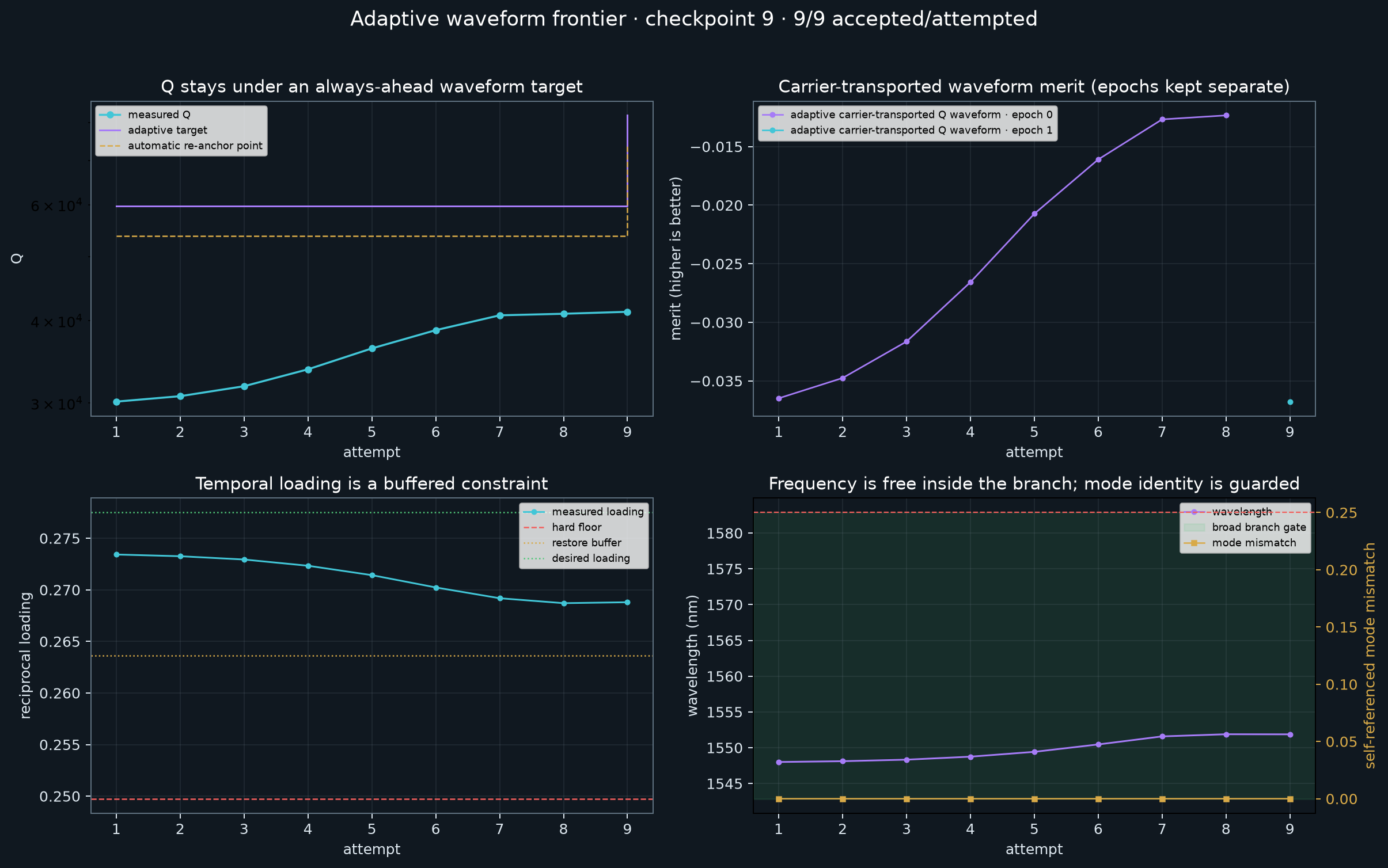
The live frontier starts from the immutable Q≈30k topology-free plateau and uses no held-out reference geometry. Its carrier-transported temporal target stays at twice the measured Q and re-anchors automatically; loading, mode identity, and broad wavelength membership are buffered constraints. Exact replay accepts every material change. The predecessor and all failed oversized escapes remain frozen evidence.
20 µm SiN/SiO2 atom gap · temporal → Q/Aeff
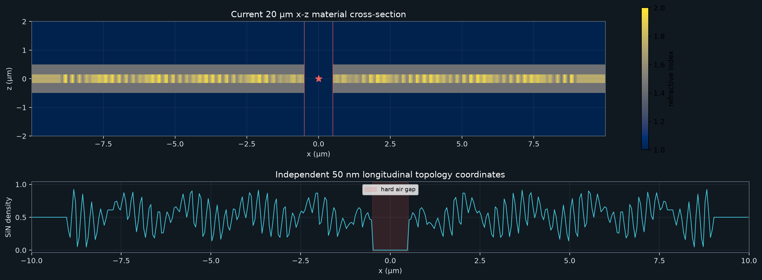
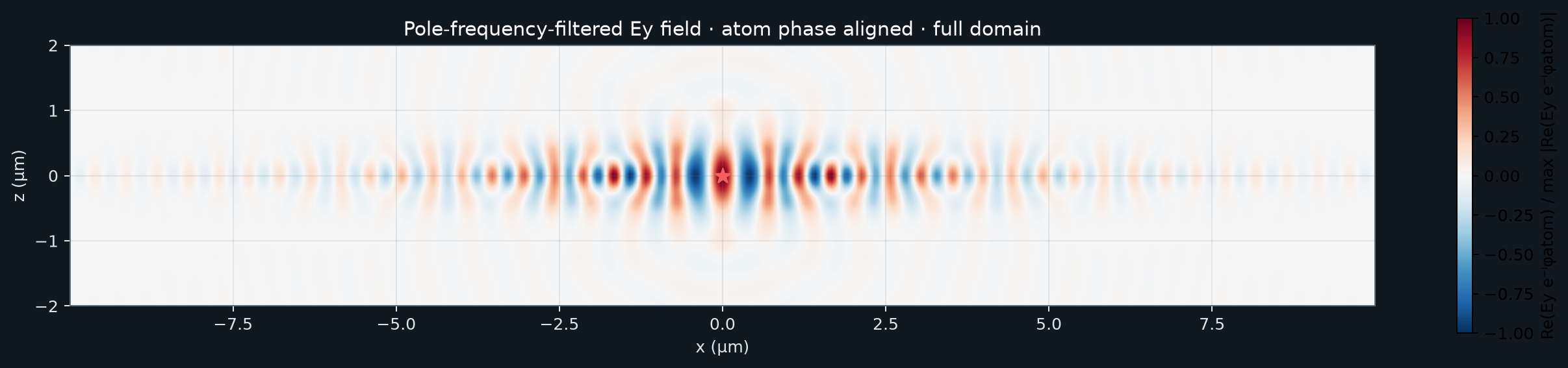
A y-invariant 300 nm patterned Si3N4 core inside a fixed 1 µm SiO2 stack, interrupted by a hard 1 µm air gap. The density-0.5 start first matches the fixed atom response to a solved inward TE-mode pulse; after a trustworthy atom pole and measured slowdown it hands off to replay-gated same-pole Q/Aeff. The field panel is pole-frequency filtered.
8 × 8 µm SiN/SiO2 atom slot · y dipole
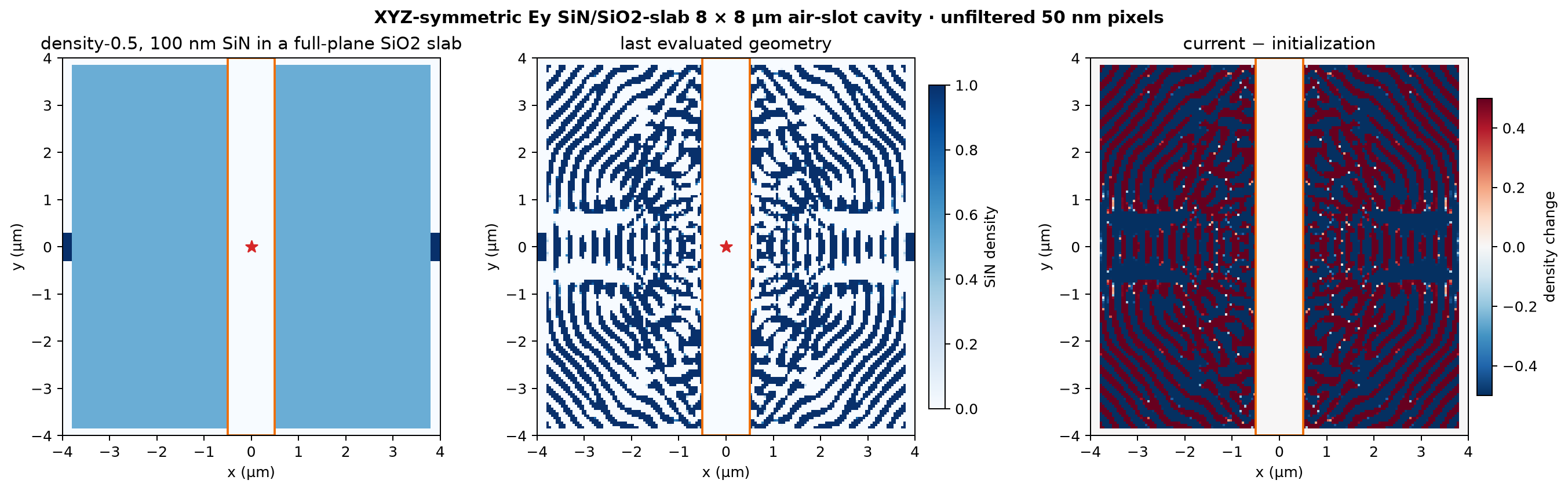
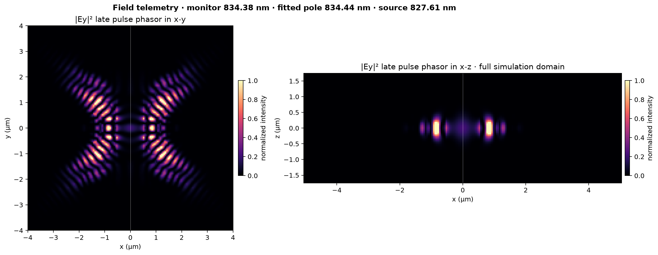
A density-0.5, component-aware Yee campaign with a hard one-micron atom strip. The SiO2 slab fills the complete x–y plane through the PMLs, while an explicit air cutout removes the entire strip. It discovers the absolute Ey temporal response, then moves through pixel-only Q, joint SiN/SiO2-thickness Q, gradual fixed-beta Q, and topology-free smooth-boundary Q. The failed z-dipole vacuum branch is preserved separately.
Composite Si₃N₄/SiO₂ waveguide · air-gap transmission
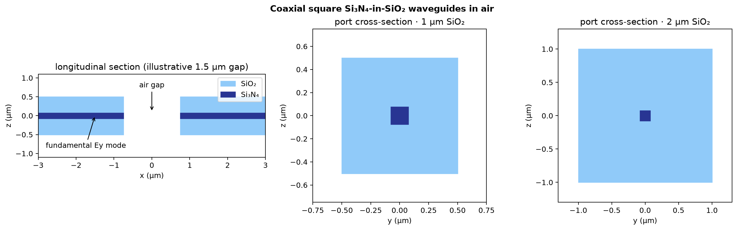
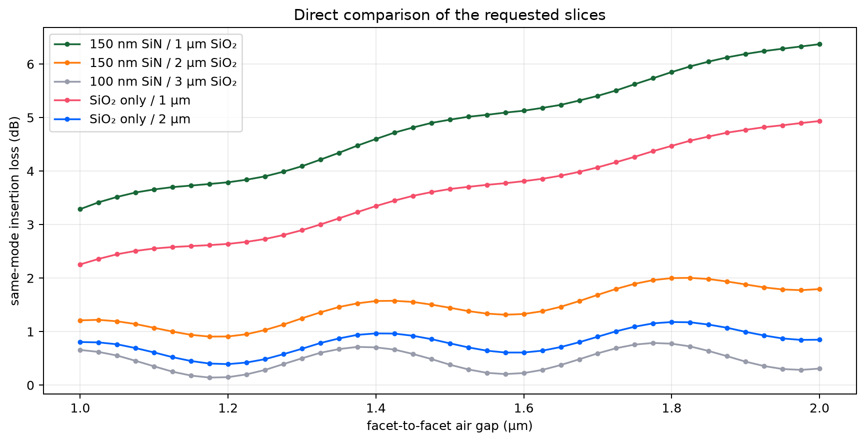
A fixed-port 780 nm FDTD sweep measures same-mode transmission, reflection, and uncollected power across 1–2 µm air gaps. It includes 150 nm Si₃N₄ cores in 1 and 2 µm square SiO₂ guides, a 100 nm / 3 µm slice, and SiO₂-only 1 and 2 µm controls. The stored tensors are ready to expand into a full three-parameter seed search.
16 × 2 µm SiN/SiO2 atom strip · variable oxide guide width
A clean successor to the live component-aware campaign. The SiN topology starts at density zero; after temporal discovery and pixel-only Q/V, SiN thickness, exact-index-1.44 SiO2 thickness, and analytic SiO2 width optimize jointly. Beta acts only on SiN, so oxide and nitride cannot collapse into an ambiguous ternary density.
16 × 2 µm SiN/SiO2 atom strip · component-aware Yee landmark
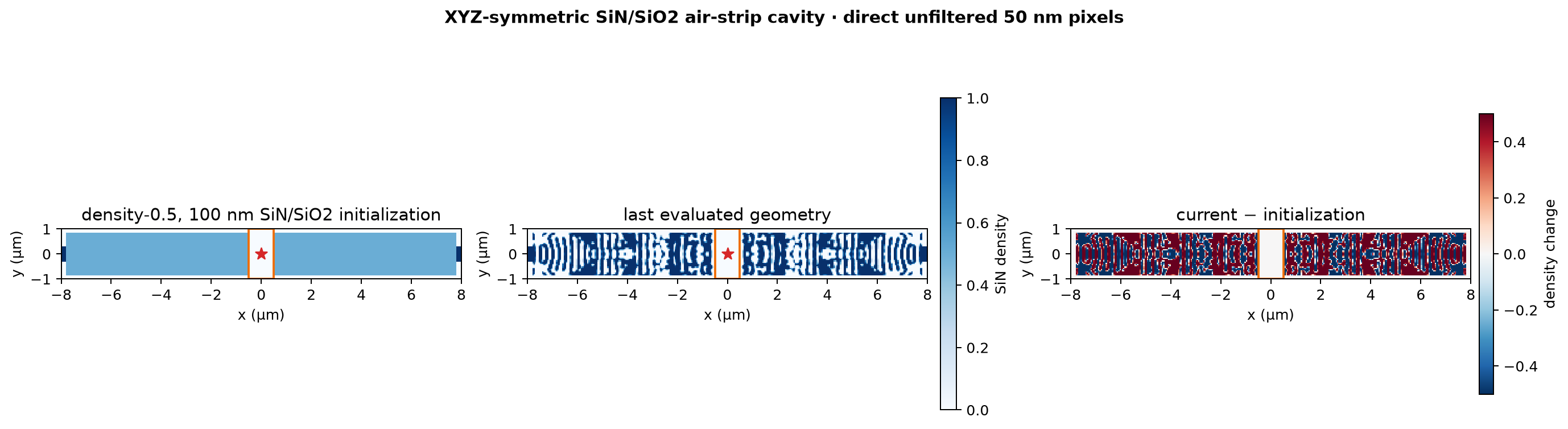
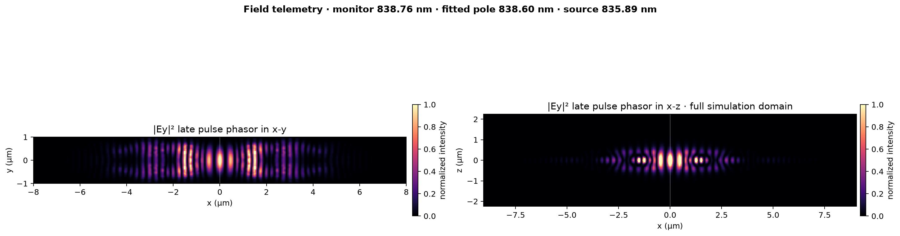
Frozen at accepted update 2562 with the one-micron atom-access strip intact. The exact final geometry gives Tidy3D Q=3,894, V=5.993 (λ/n_air)³, Q/V=649.8, Purcell=49.38, and λ=826.21 nm; the same checkpoint gives FDTDX Q=5,807, V=4.612, and Q/V=1,259. The complete optimizer state, smooth boundary, validation record, and immutable success archive are preserved for later continuation.
16 × 2 µm, 100 nm SiN in SiO2 · xyz-symmetric y atom
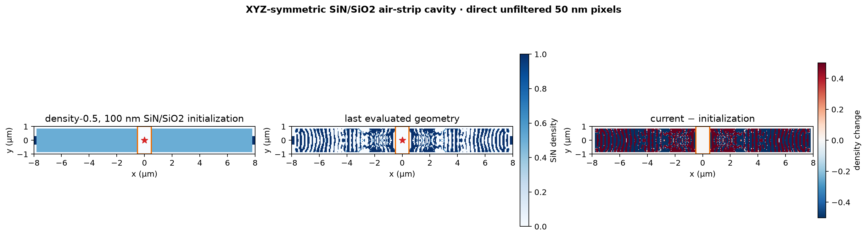
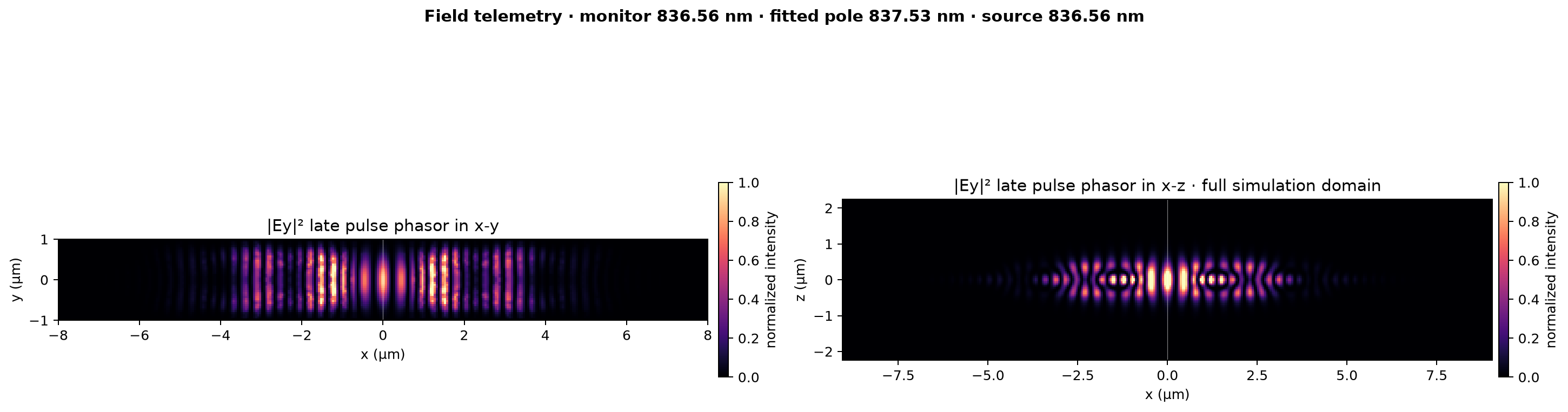
The original density-0.5 campaign is preserved at accepted update 583 for comparison. Its scalar-material FDTDX result motivated the independent Tidy3D validation and the component-aware Yee restart above; it is no longer the running optimizer.
16 × 2 × 0.5–0.7 µm SiN atom strip · xyz-symmetric y atom
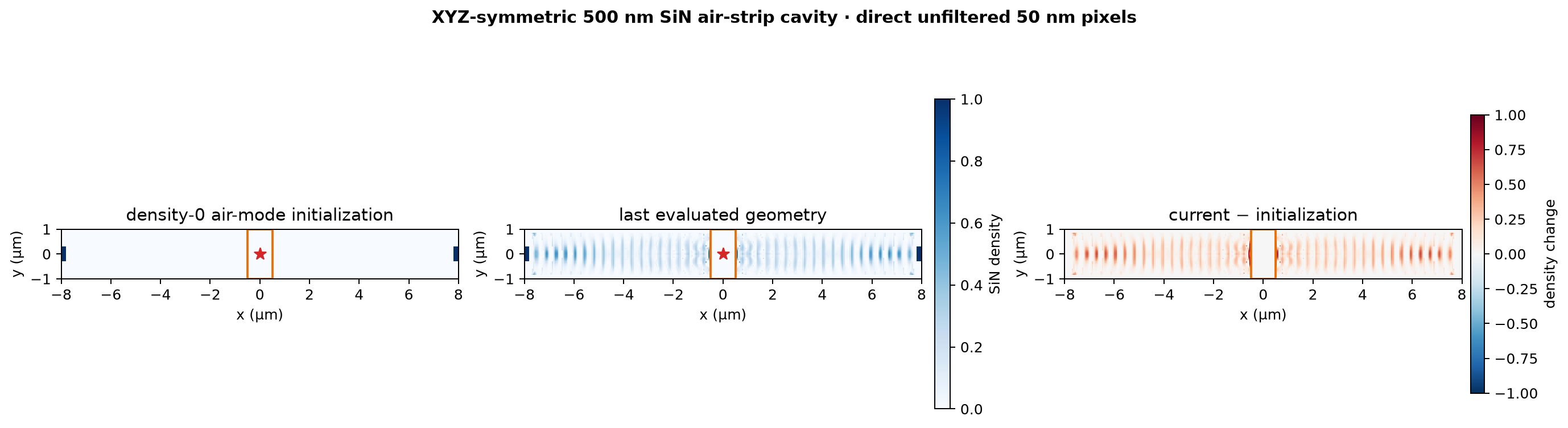
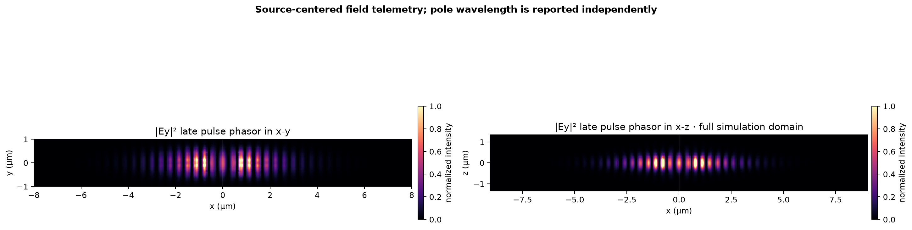
Paused at trustworthy Q=1,978, V=4.210 λ³, Q/V=469.9, and atom-local Purcell=35.71 after 118 accepted pole updates. Its frozen-volume Q controller ultimately reached a trust-floor plateau; the exact full-state checkpoint and immutable qualified-success archive are preserved.
12 × 4 µm SiN atom hole · xyz-symmetric y atom
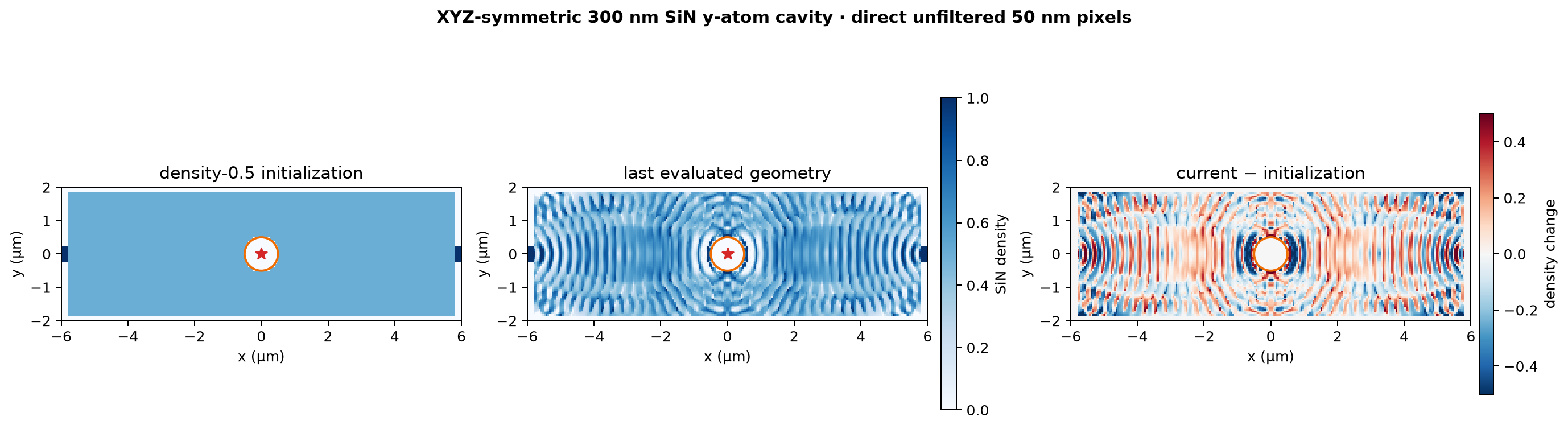
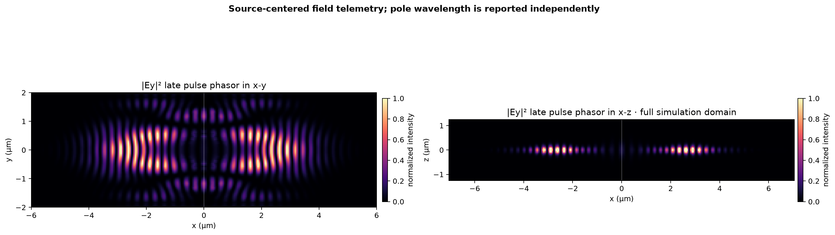
Paused at trustworthy Q=10,057, V/λ³=61.24, atom-local Purcell=12.49, and 48.70× the handoff reciprocal guided-Purcell proxy; best observed Q was 10,499. The useful coupling gain is a qualified success, while the dielectric-centered mode and excessive Q requirement motivate the air-strip successor. Its exact optimizer state and hash-addressed checkpoint are preserved.
300 nm SiN z-atom hole · one-sided V-constrained Q
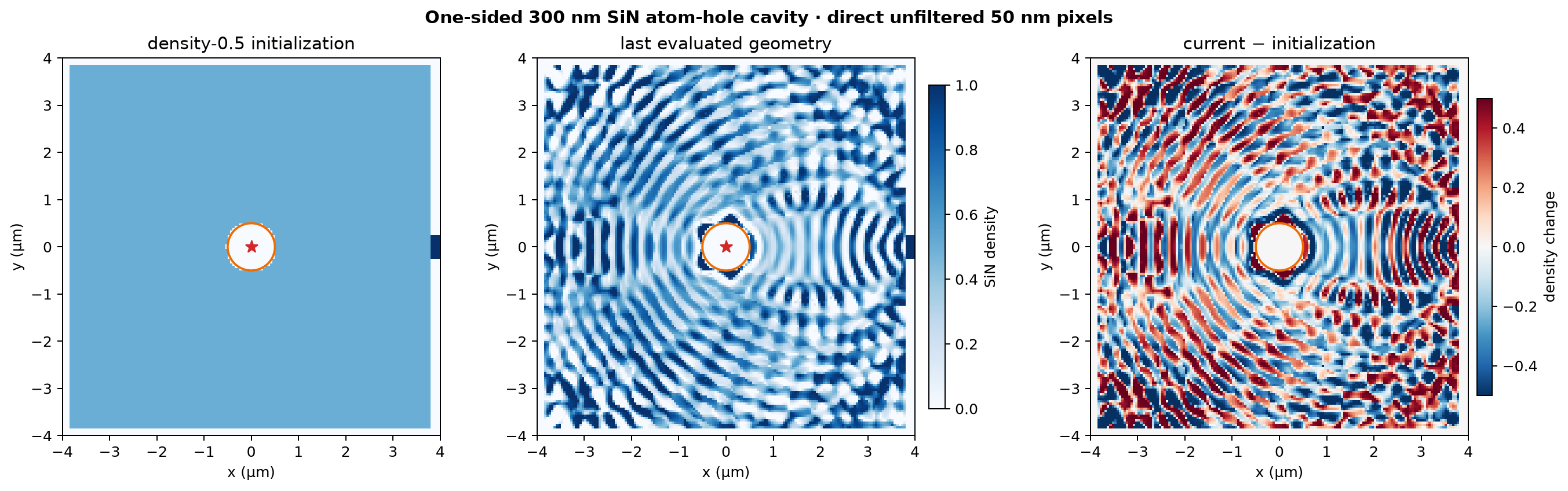
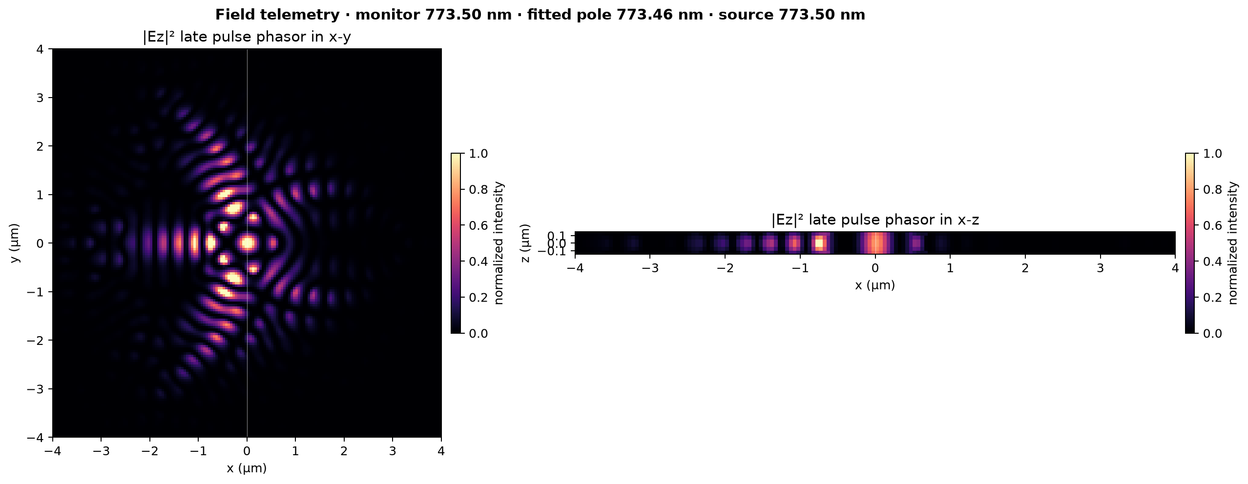
The corrected one-sided branch reached Q=1,767 with physical atom volume 1.940 µm³ below its frozen 2.068 µm³ ceiling. Its exact optimizer state, cached trust controller, and immutable hash-addressed checkpoint are preserved for later continuation.
Fryett 16 µm nanobeam · extended-mirror lifetime

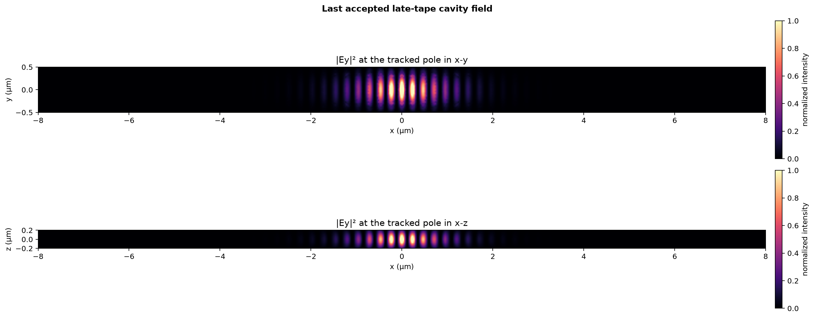
The successful temporal-to-pole sequence reached Q=6,322 in 8 µm, inferred and repeated its learned 256.589 nm outer mirror cell through a 16 µm fork, and climbed from an independently audited Q=42,361 seed to Q=138,284. The exact unbinarized 25 nm checkpoint is preserved for later binarization and smooth-boundary continuation.
Fryett nanobeam · symmetric ports → central dipole
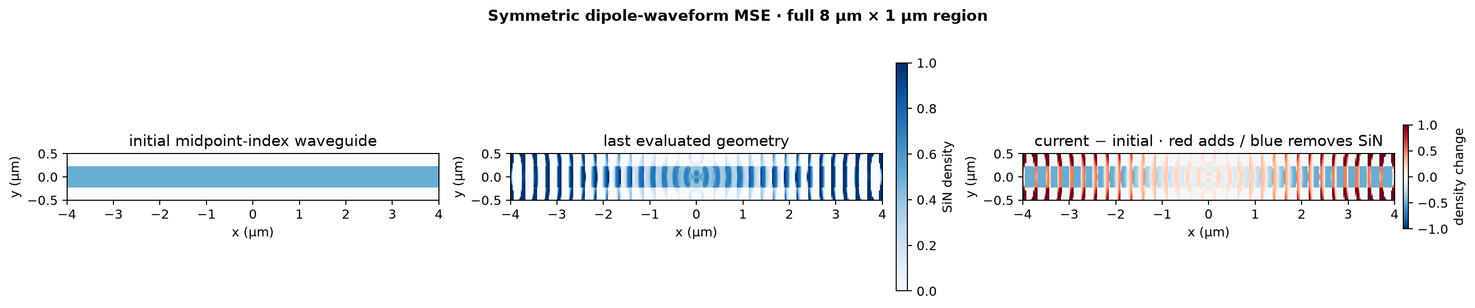
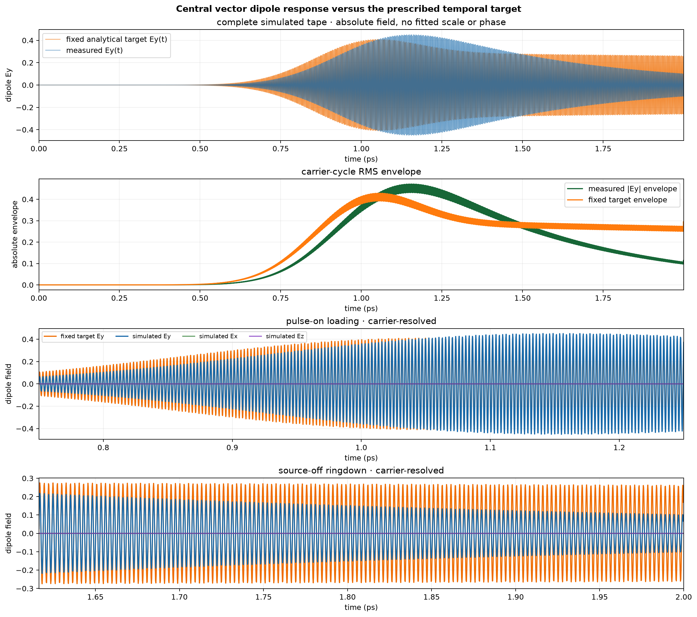
An x/y/z-symmetric unit-power bright TE port pair drives a central y dipole. The sole objective is full-vector temporal MSE against a fixed 780 nm, Q=10,000, V=0.1 um3 analytical response. Each raw Adam update is one 2 ps forward/adjoint pair over 3,200 independent 25 nm density pixels; Q, V, and two-port beta are telemetry only.
Fryett nanobeam · pulsed midpoint-guide/source Adam
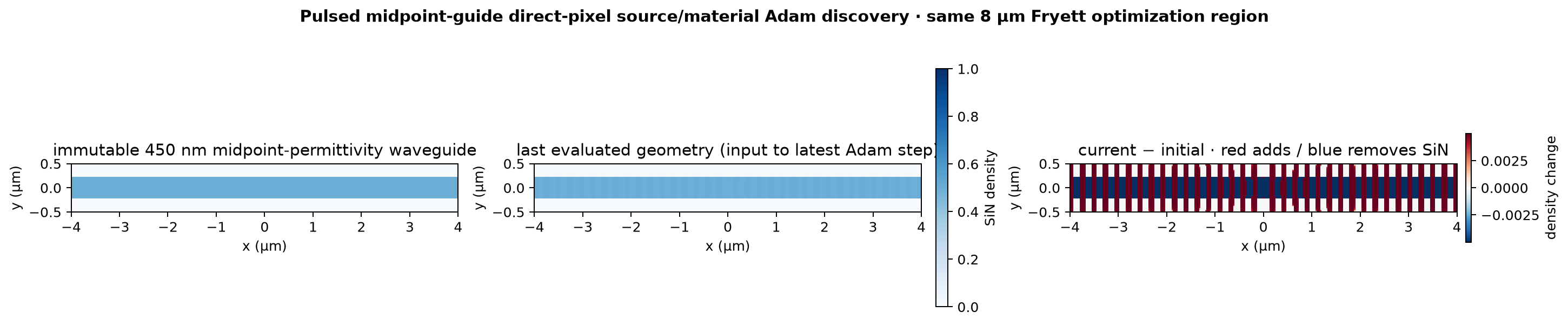
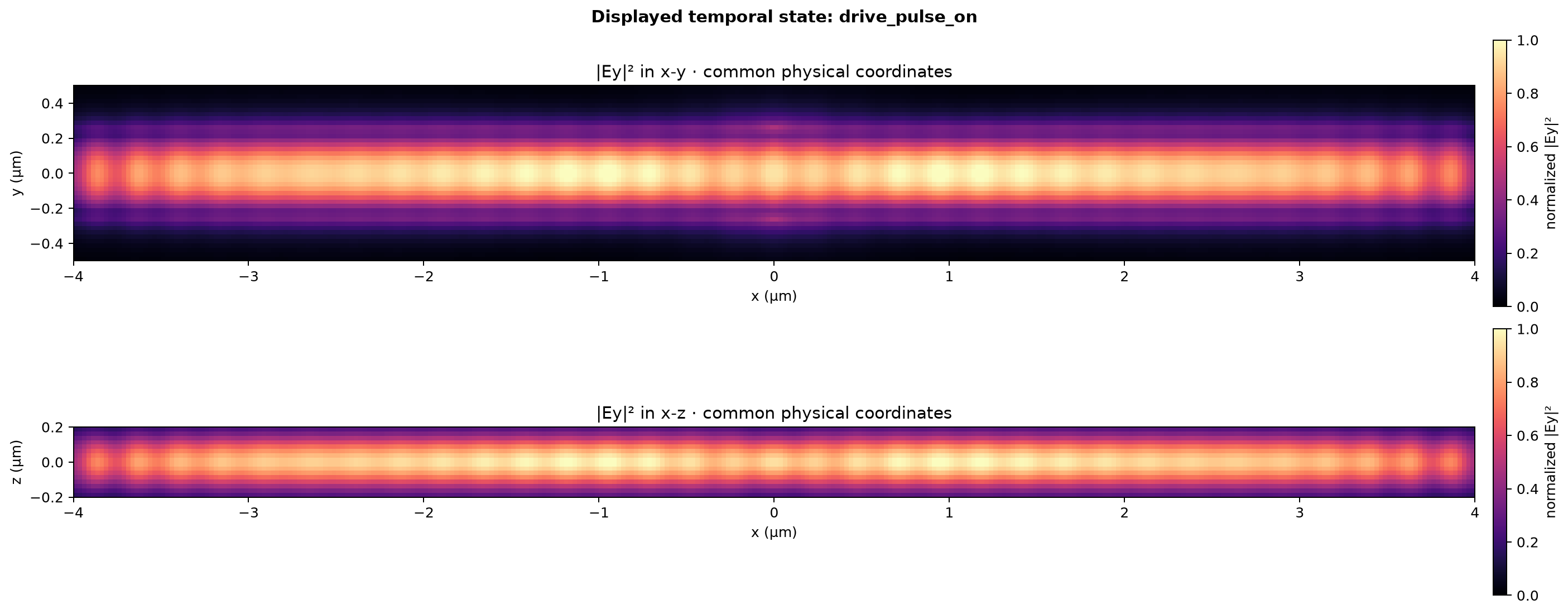
A broadband Gaussian pulse replaces the CW-like burst. Direct 25 nm pixels start as a density-0.5 midpoint-permittivity waveguide and its solved fundamental mode source. The ideal target is recomputed as the exact causal pulse convolution with a unity-amplitude lossless cosine pole. One reverse pass returns both gradients and commits one unconditional Adam step.
Fryett nanobeam · unbinarized source-equilibrated discovery
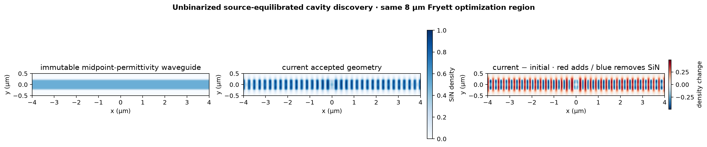
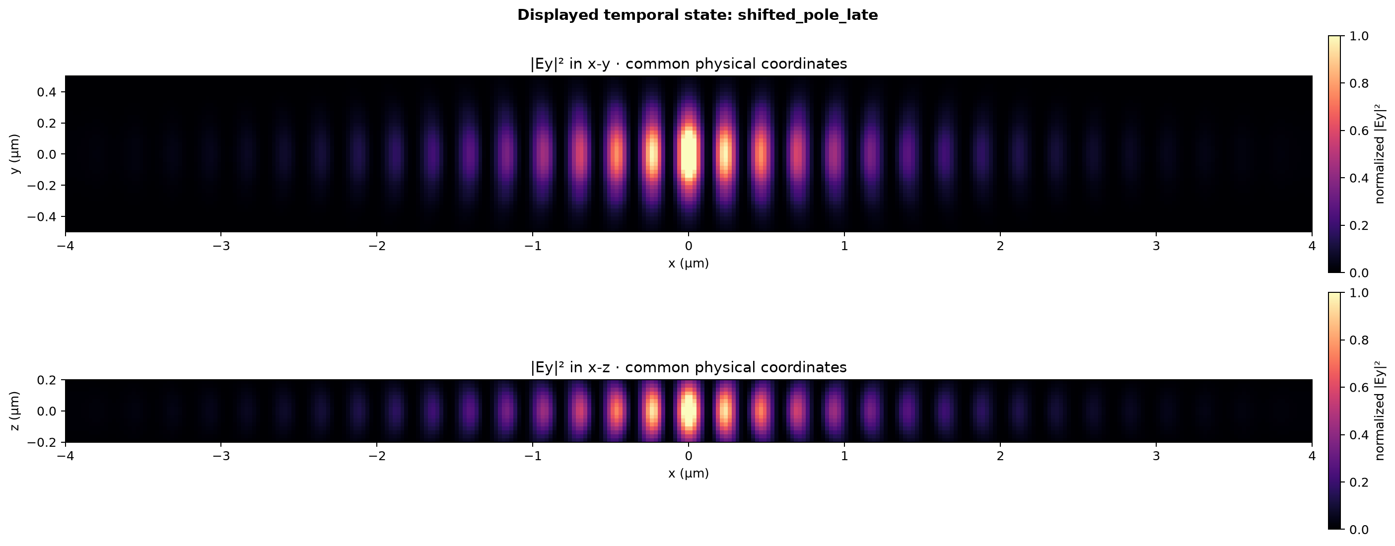
A fresh midpoint-guide campaign keeps continuous filtered density forever—no projection, beta schedule, binary pressure, or boundary handoff. The 2,700-coordinate source is locally equilibrated around every material decision while agreement-controlled trust radii grow without a scheduled release.
Fryett nanobeam · frozen evolved source → smooth boundary
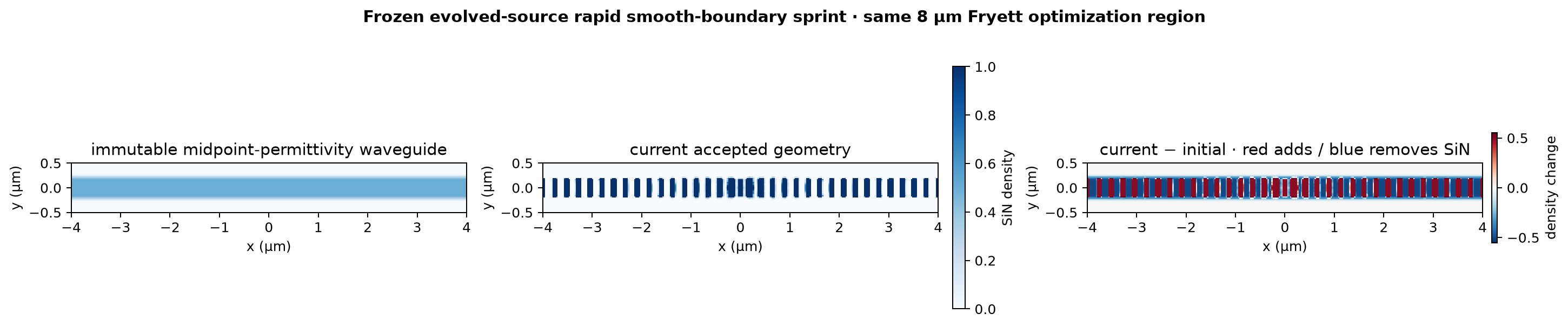
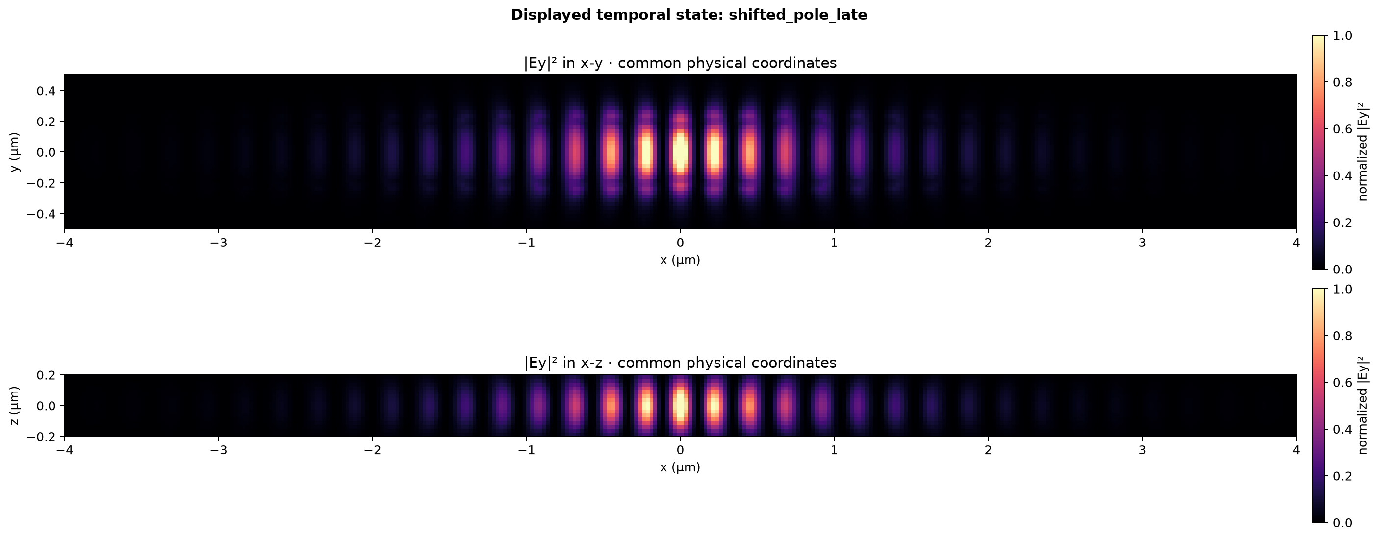
A rollback-safe fork freezes the evolved source, jumps directly to beta 64, and removes all source inner solves. Direct material trust-region steps rapidly test the present architecture before fail-closed replay into a smooth subpixel level-set boundary.
Fryett nanobeam · source-equilibrated dielectric
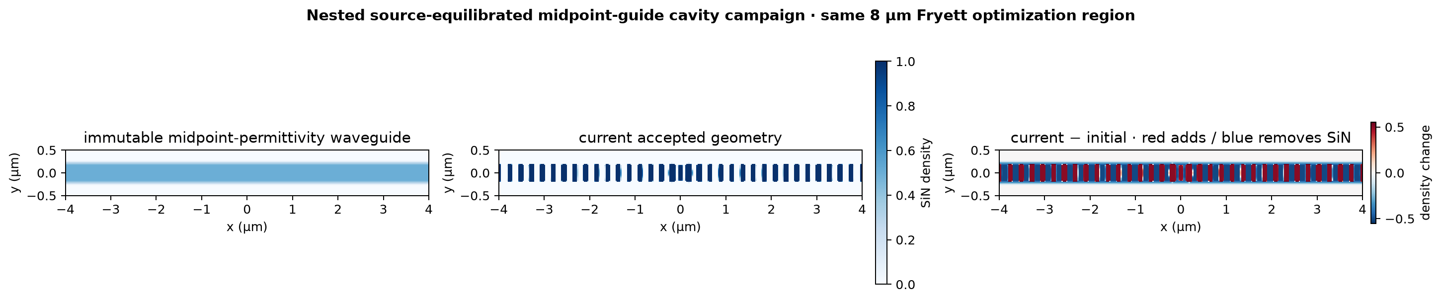
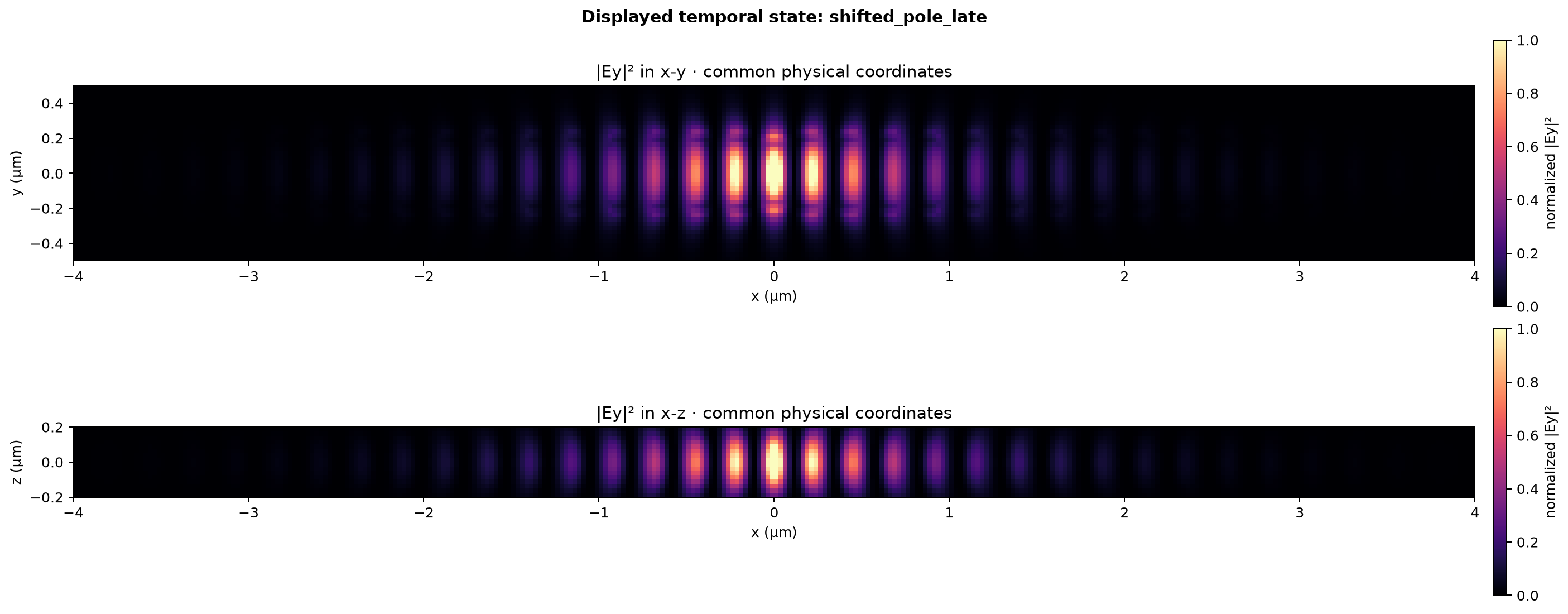
A nested variable-projection successor starts from a 450 nm midpoint-permittivity guide in a 1 µm-wide region and equilibrates all 2,700 fixed-norm source coordinates before every material decision. Density trust and beta release slowly over accepted commits, then a stable beta-64 topology replays into a smooth cut-cell boundary.
Fryett nanobeam · reciprocal modal current
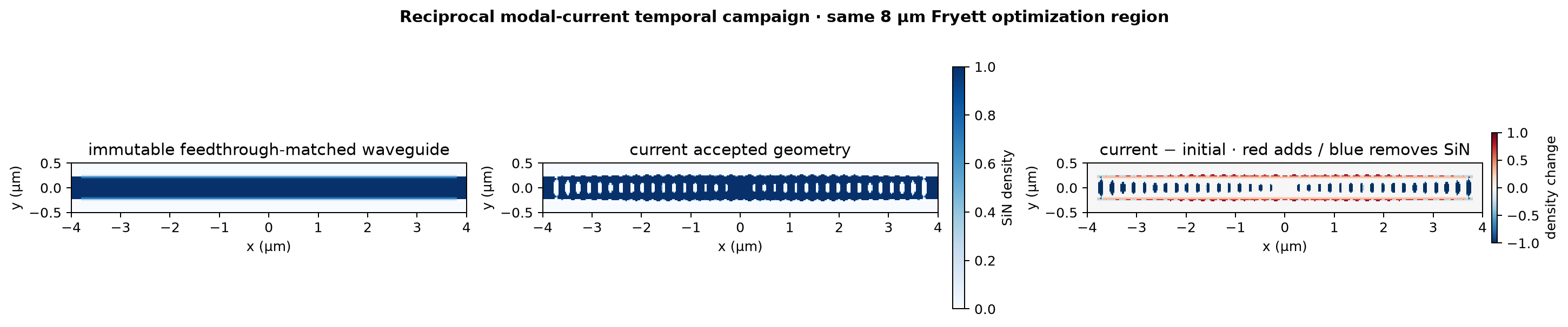
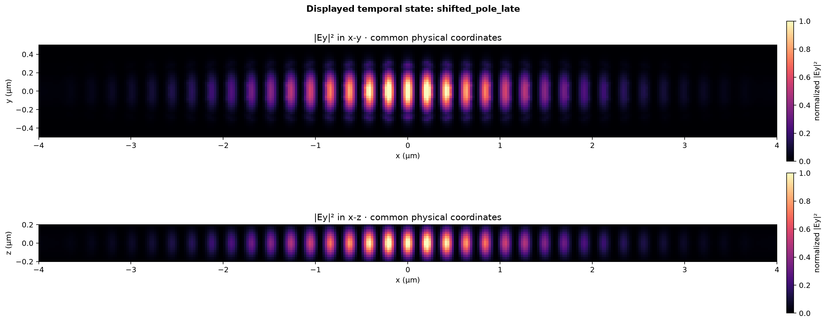
A fixed fundamental-TE feedthrough profile is used as both the centered bidirectional electric current and its reciprocal scalar observable. One absolute causal lossless waveform drives the complete optimization, with Q≥100 pole tracking and a replay-gated smooth-boundary handoff.
Fryett nanobeam · joint dielectric and source
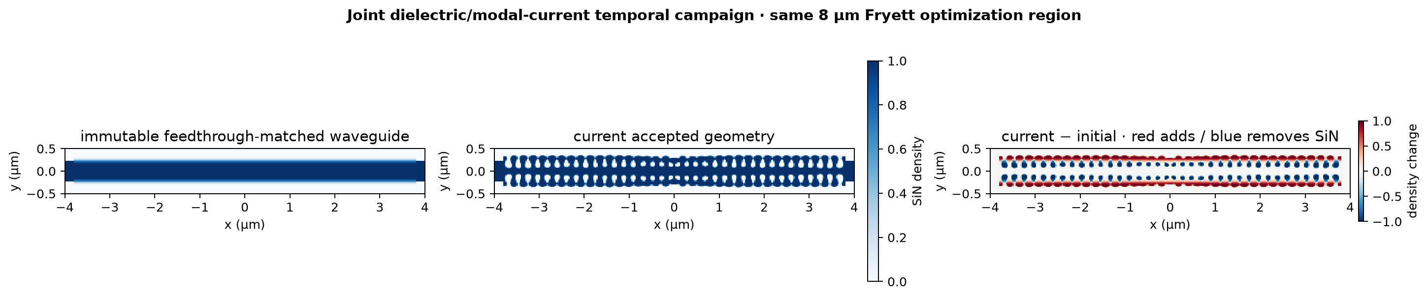
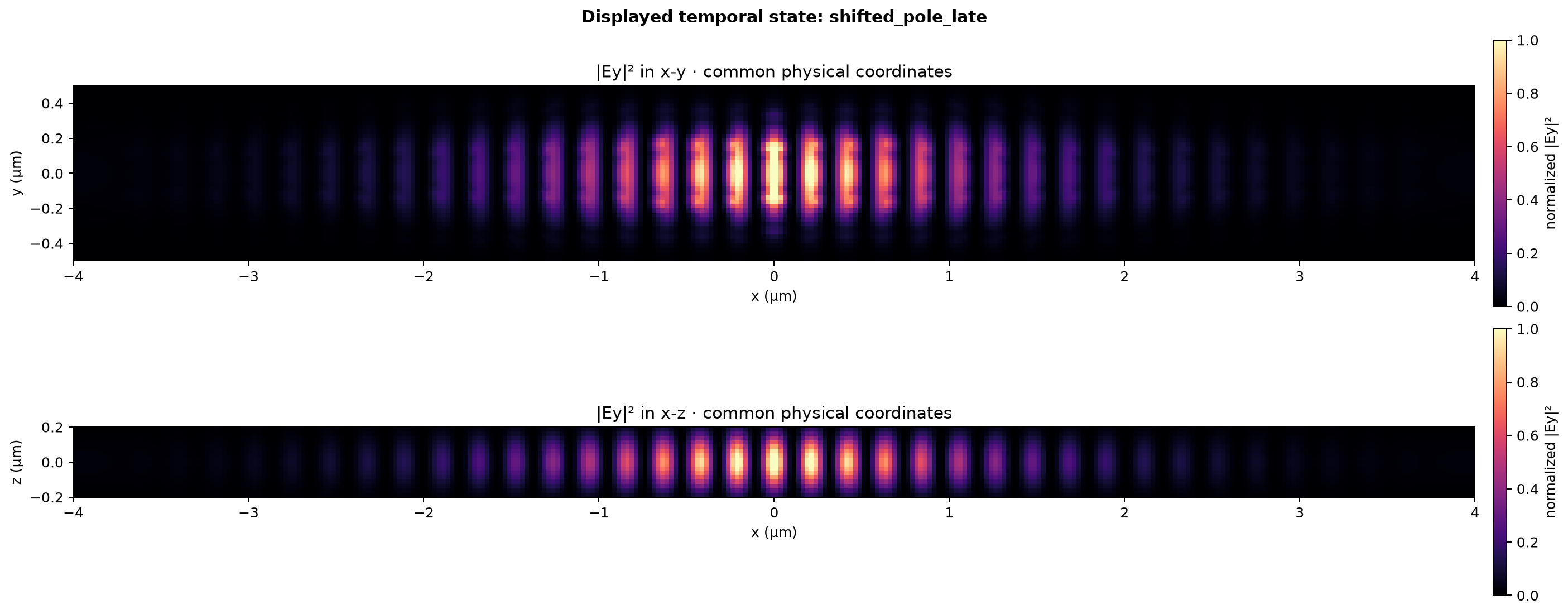
The fixed-waveform successor exposes all 2,700 physical transverse Ex/Ey/Ez source samples at fixed norm. Its dielectric is a topology-free cubic-spline phase field whose sharp limit is binary bulk plus physical gray cut cells on one continuous boundary; one reverse pass drives both trust-region L-BFGS blocks.
Fryett nanobeam · lossless temporal target
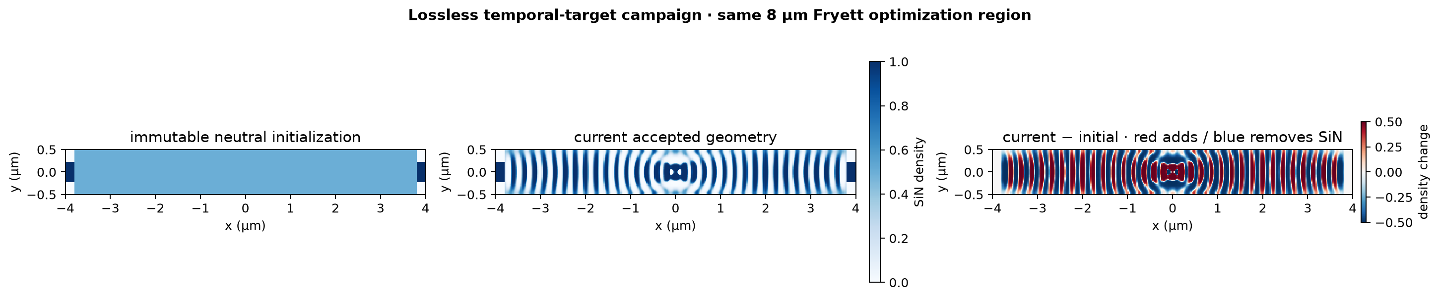
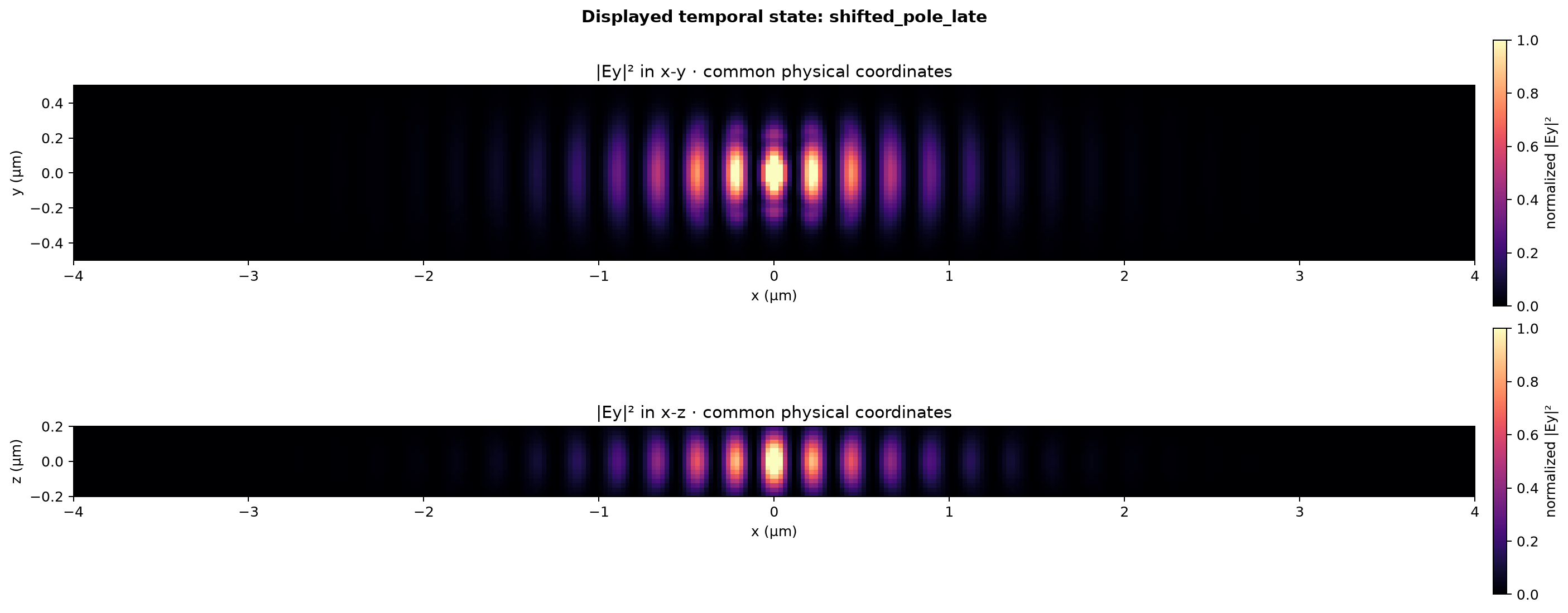
One objective from the neutral start rewards the exact source-driven lossless single-pole waveform. Raw pixel gradients rapidly binarize, a trustworthy Q≥100 pole enables carrier tracking, and a replay-gated level set takes over at the mature boundary.
Fryett nanobeam · full-field 4D Q/V
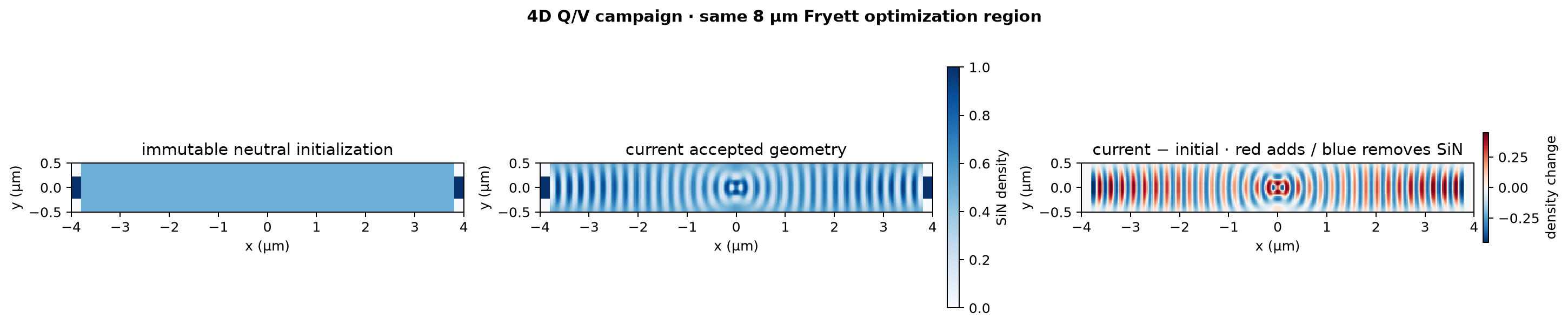
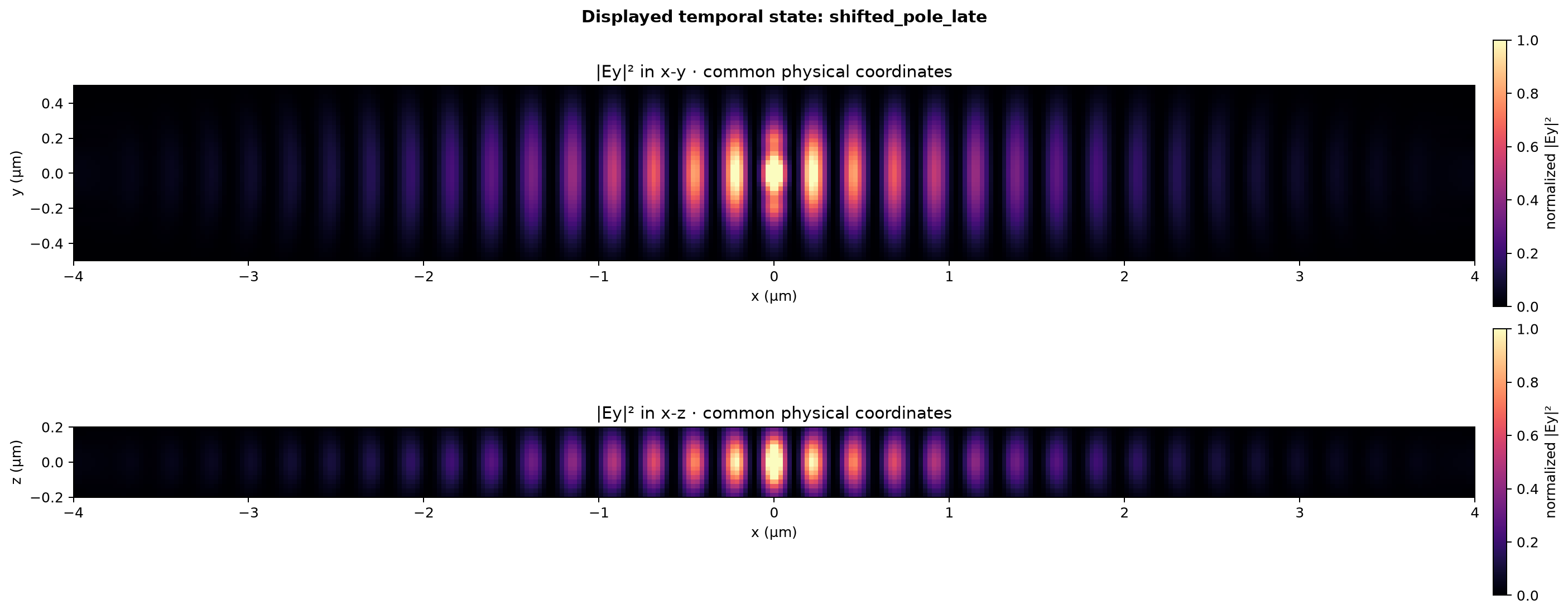
All 3,200 design pixels participate from initialization. Pulse-on-assisted discovery gives way to a fail-closed pole capture and eigenfrequency-shifted Q/V objective built from six-component fields in multiple time windows.
Fryett nanobeam · antenna first, cavity second
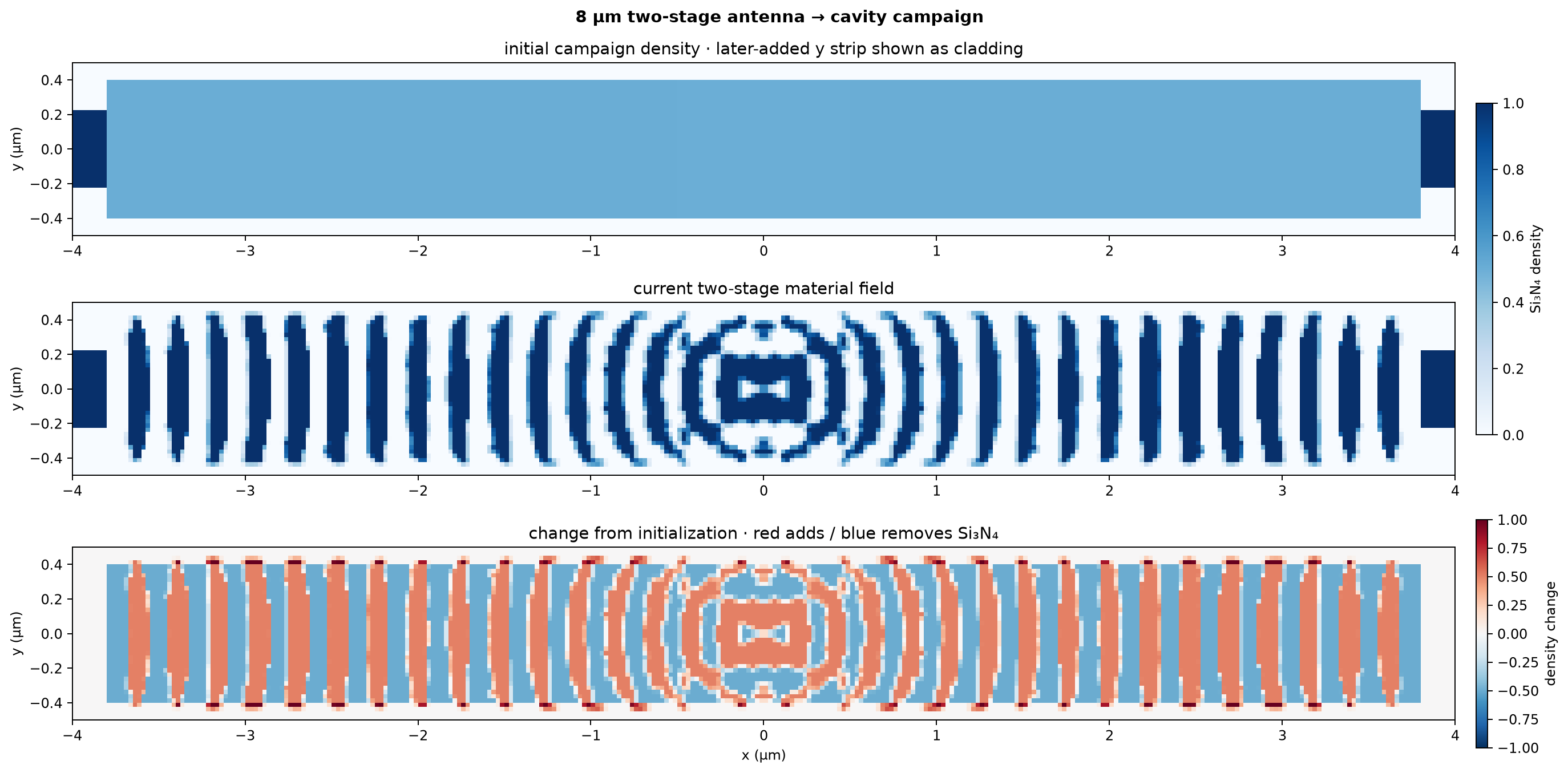
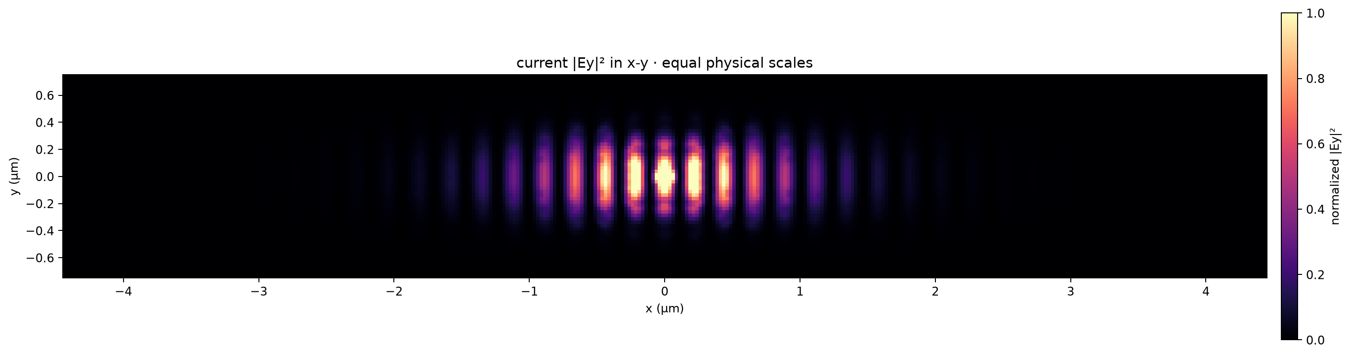
Stage 1 gives LDOS only a 1 µm, 320-pixel antenna box. After the antenna is frozen, Stage 2 activates 234 collective Bragg controls for Q growth and dark-state refinement.
Fryett nanobeam · parametric → fixed-LDOS boundary
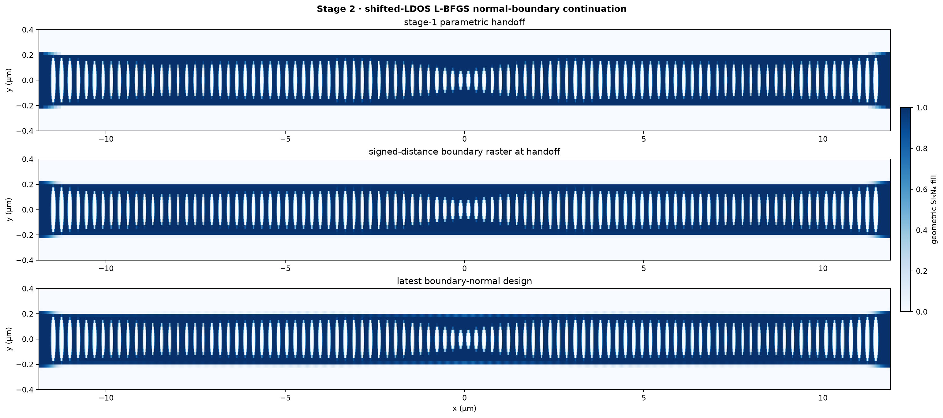
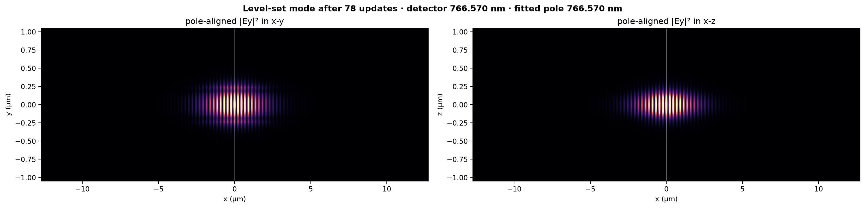
Frozen 151-parameter ellipse discovery followed by topology-preserving normal-boundary optimization of LDOS at the immutable 780.550 nm emitter line.
Device 23 · anthracene LDOS
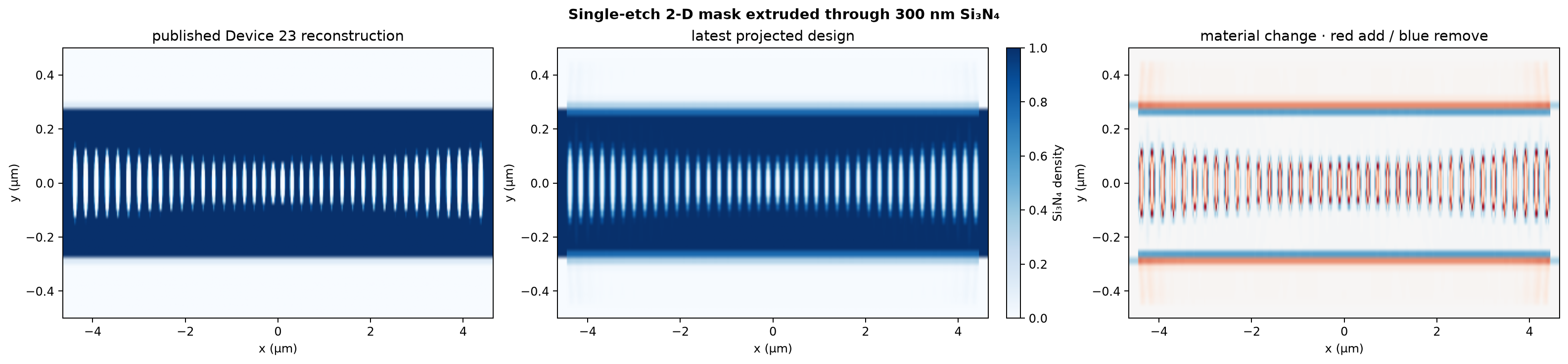
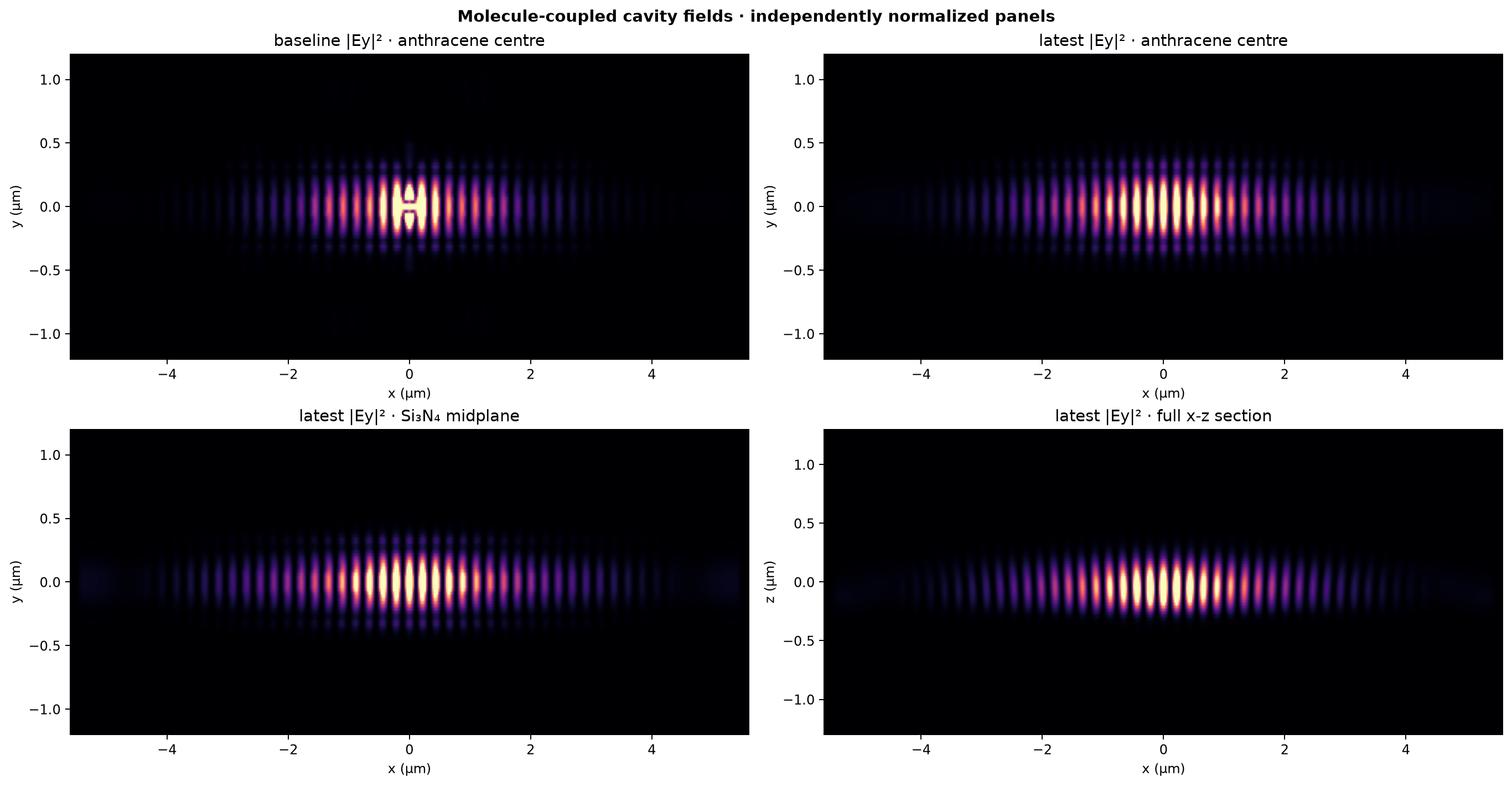
Pixelated Si₃N₄ cavity below anthracene/PVA, driven by an Ey molecular emitter and optimized through shifted Q/V.
150 nm SiN · Fourier-to-pixel
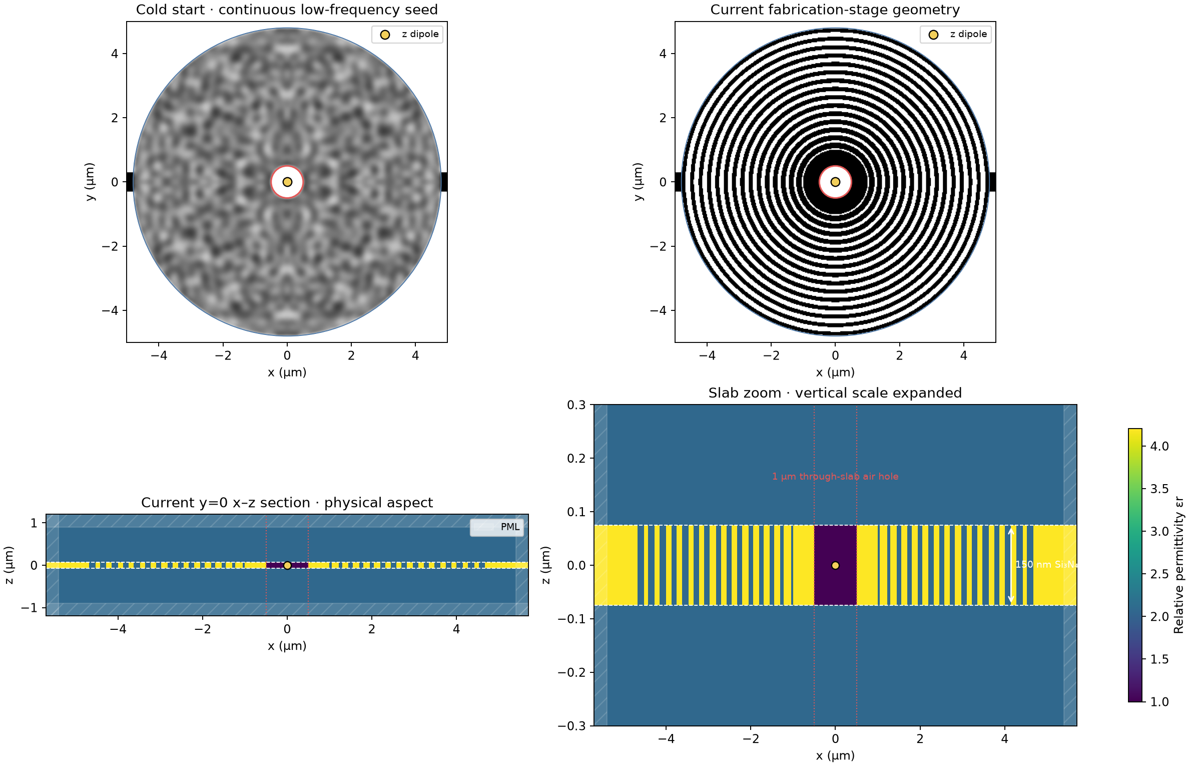
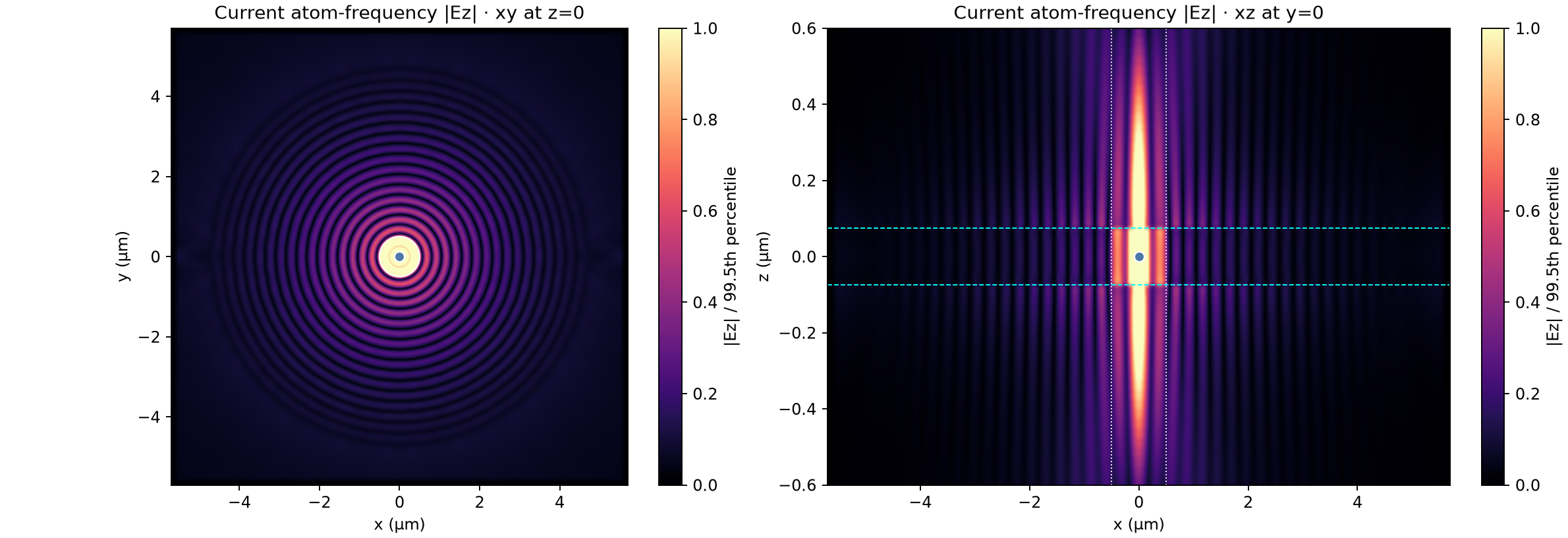
Large isotropic spectral discovery followed by exact pixel handoff and 1,283 total updates around a protected atom hole.
200 nm SiN · isotropic Fourier
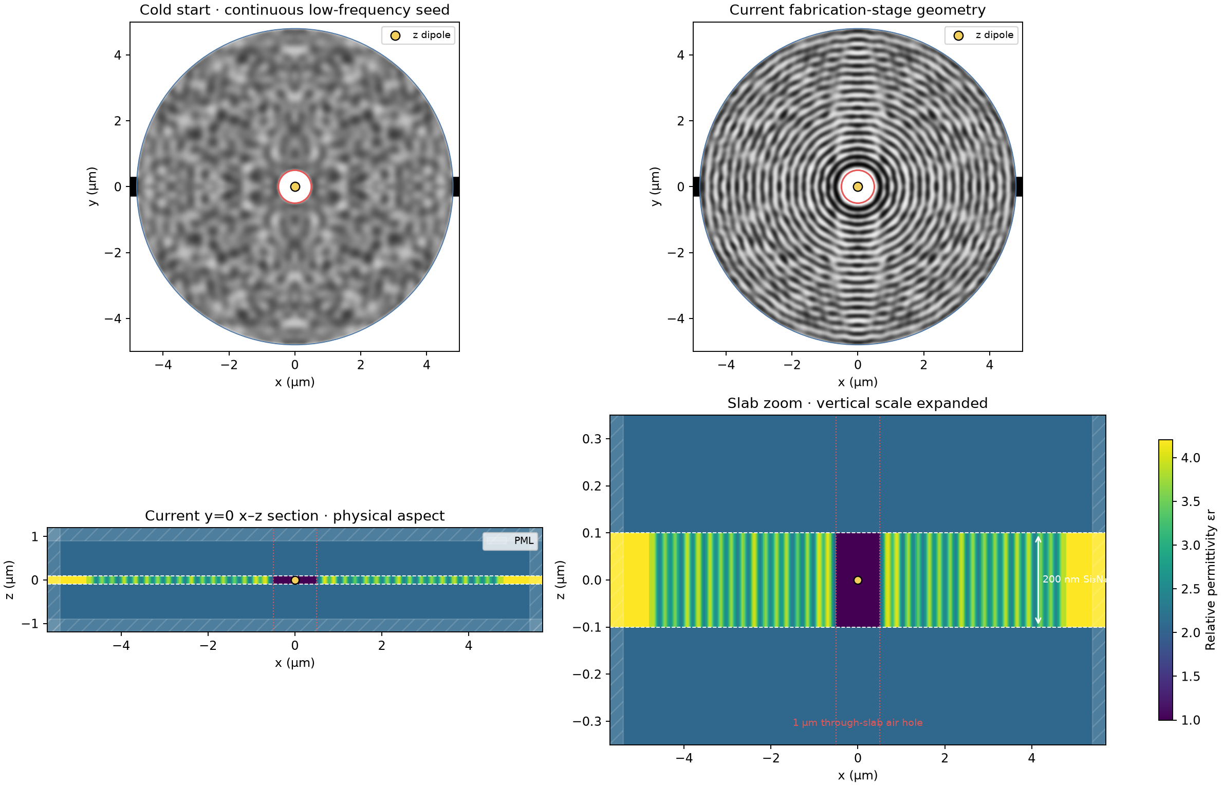
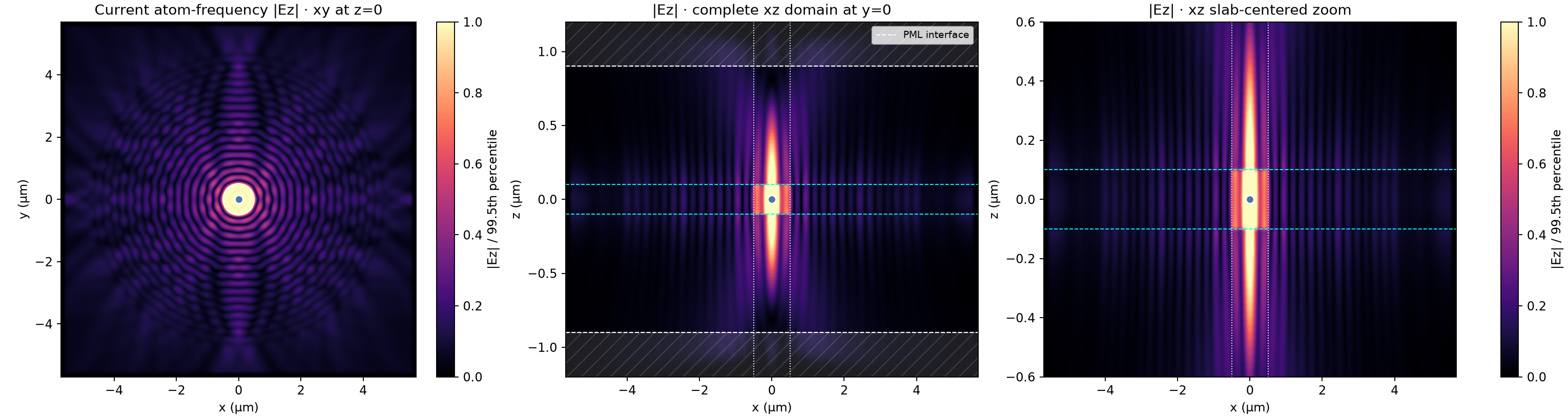
Thin-slab thickness experiment with full x-z field inspection and an independently doubled vertical-domain audit.
Axis-biased Fourier seed
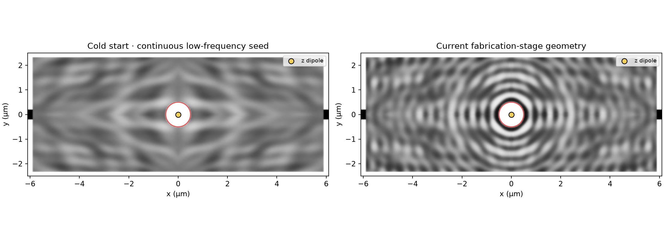
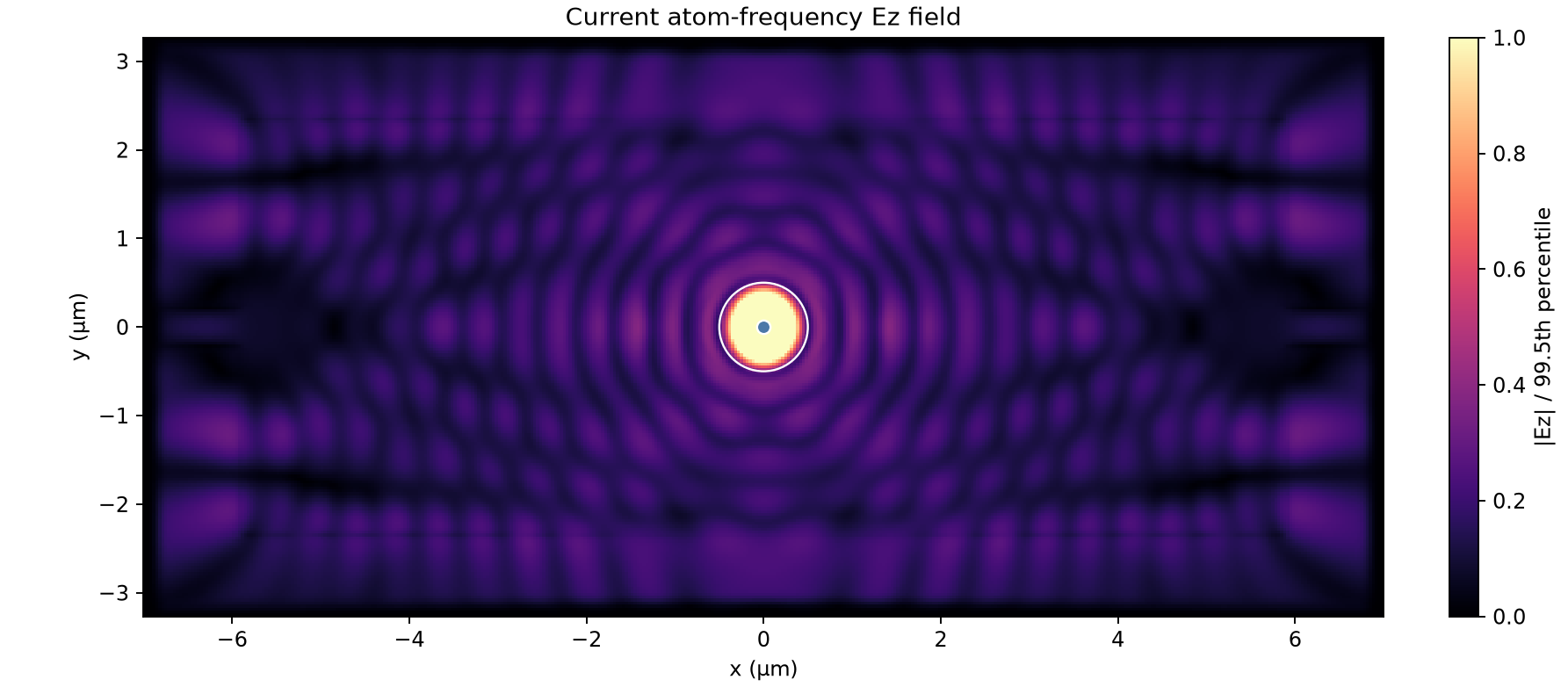
Twenty-update diagnostic exposing why the earlier spectral seed activated kx- and ky-aligned waves disproportionately.
Solid-start Fourier atom hole
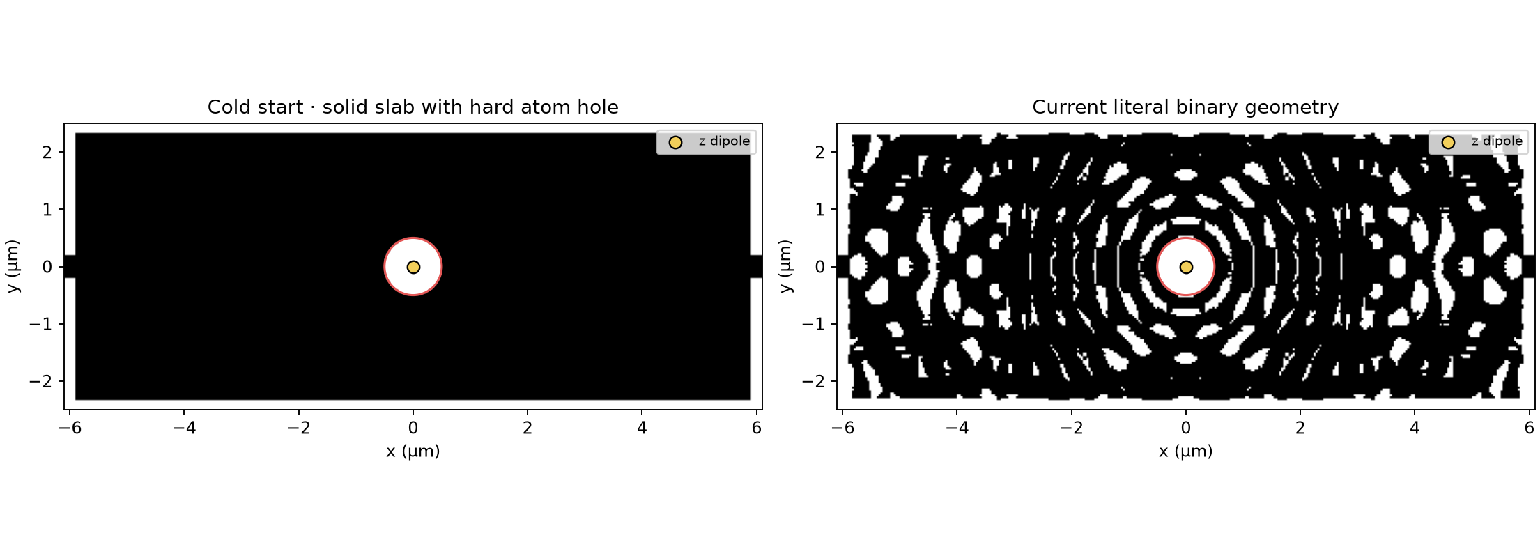
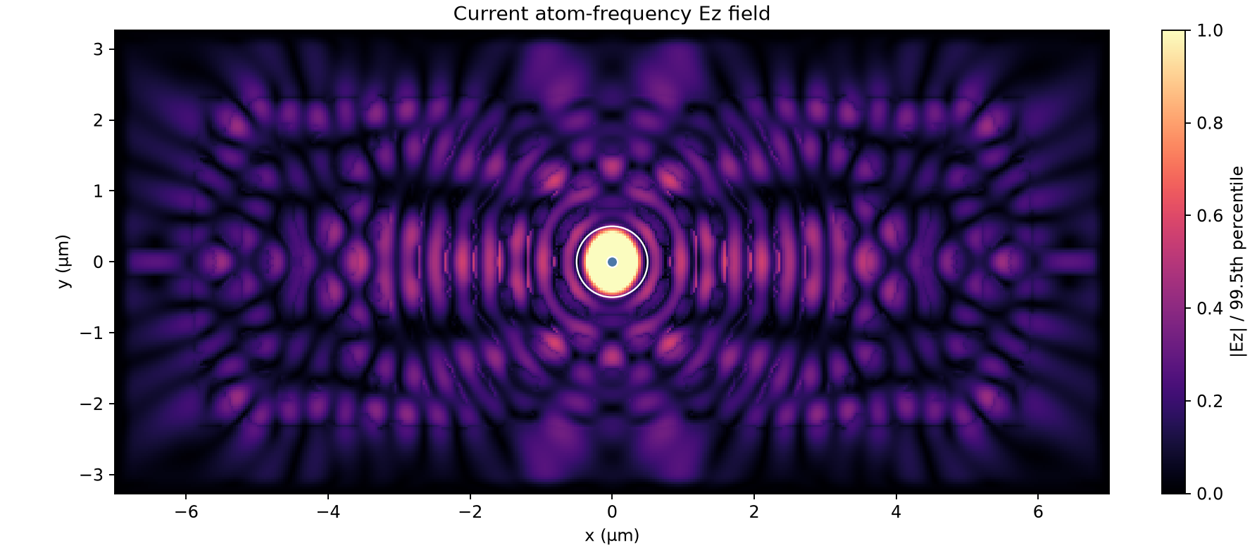
The 665-update solid-slab initialization study that motivated gradual, isotropic spectral discovery.
SiO₂-clad 250 nm SiN · spectral LDOS
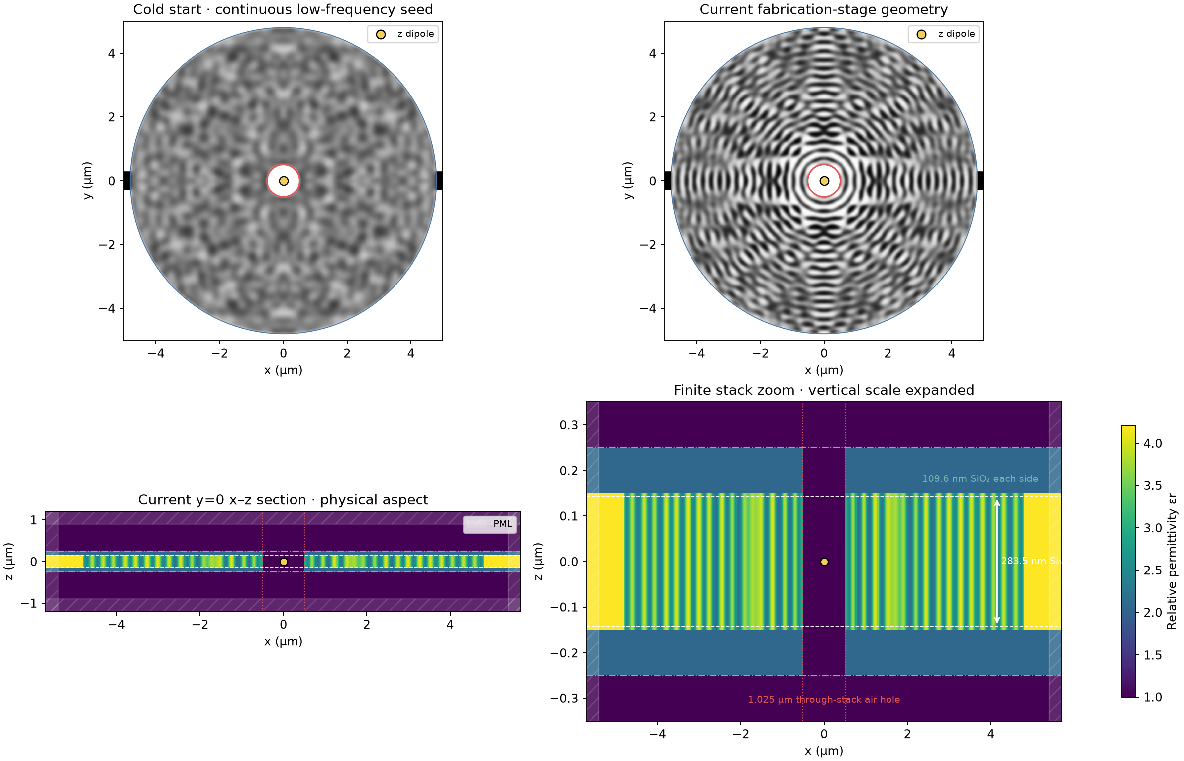
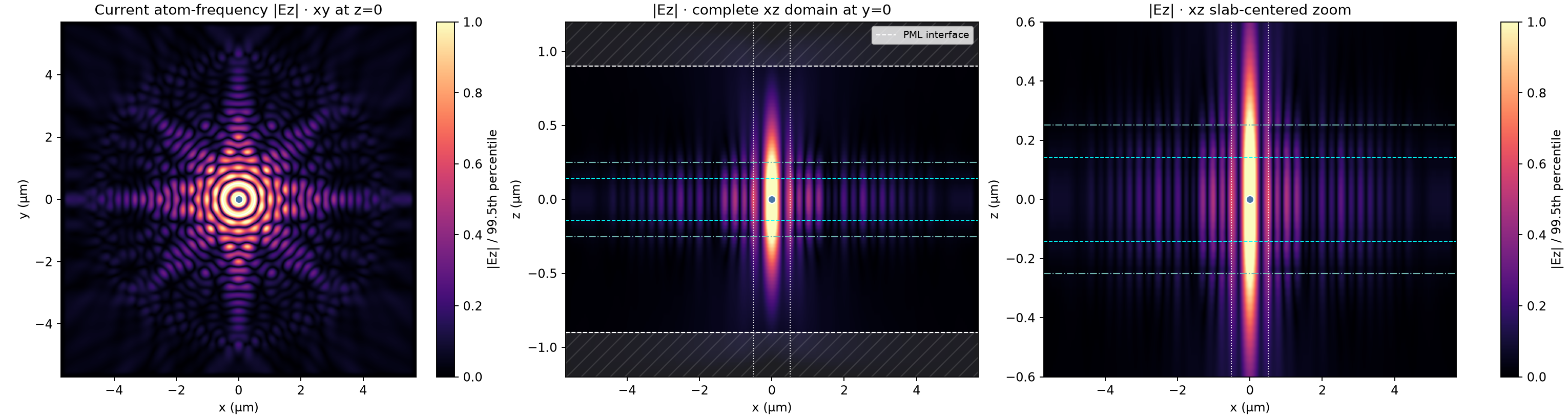
Forty-thousand-coefficient Fourier mask with differentiable SiN and symmetric SiO₂ thickness controls.
12-front curved mirrors · beta
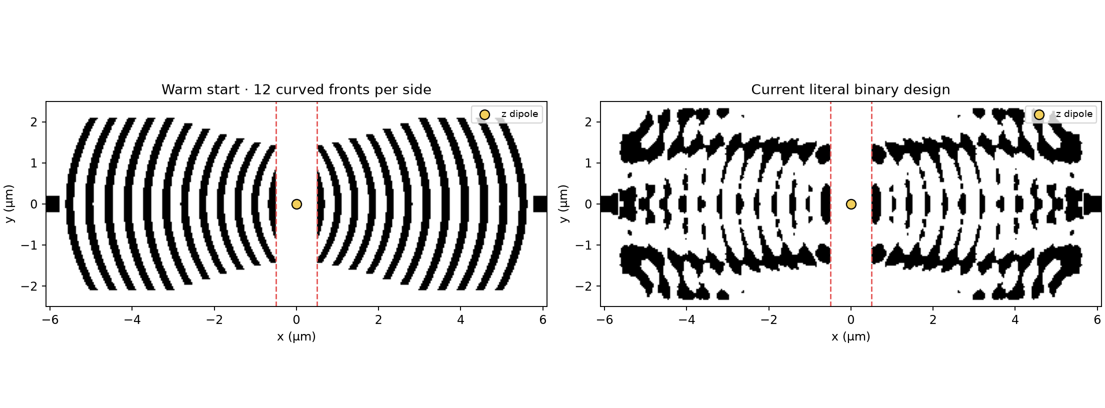
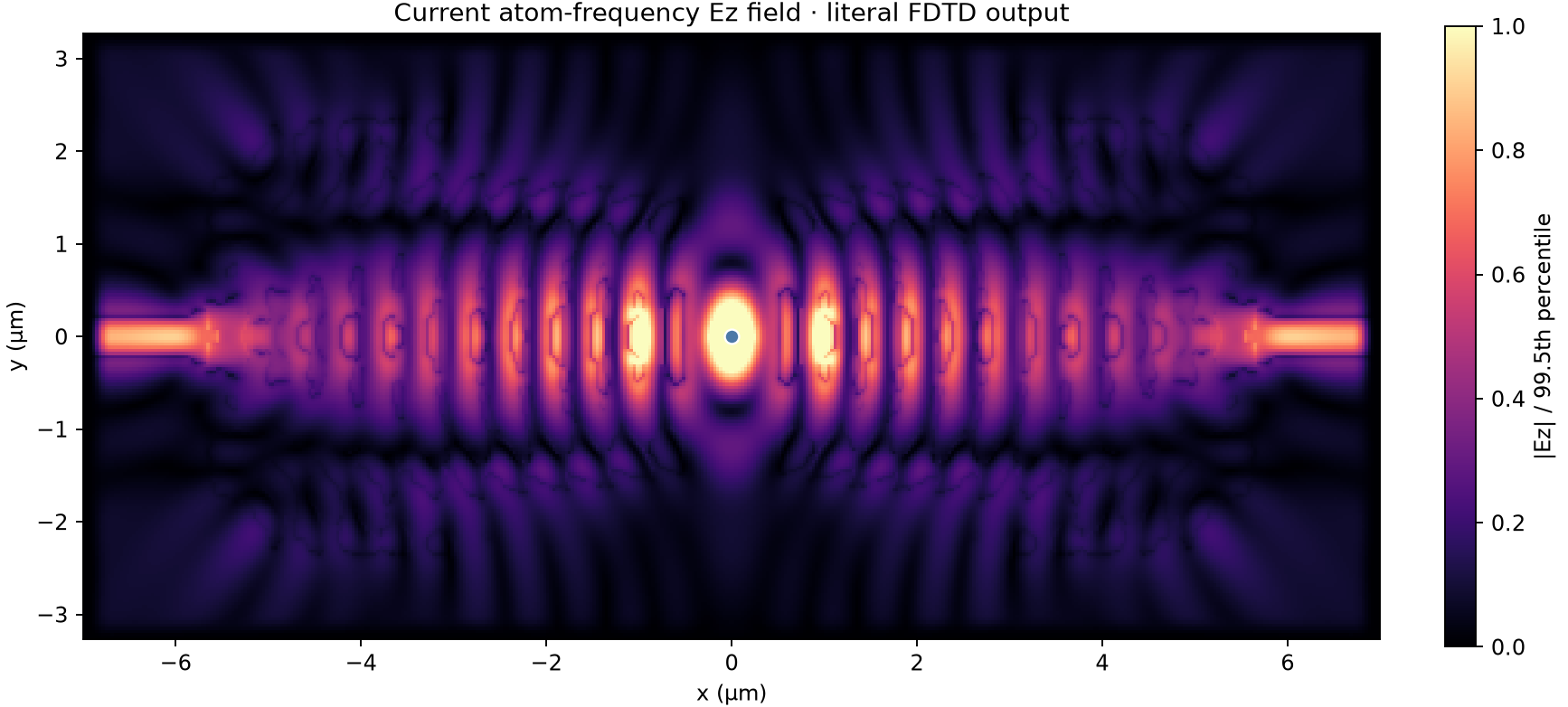
Pixel-polished facing mirrors with a frozen 53.13% two-guide coupling result and full channel accounting.
12-front curved mirrors · LDOS
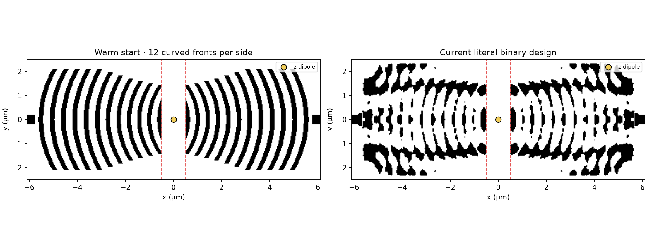
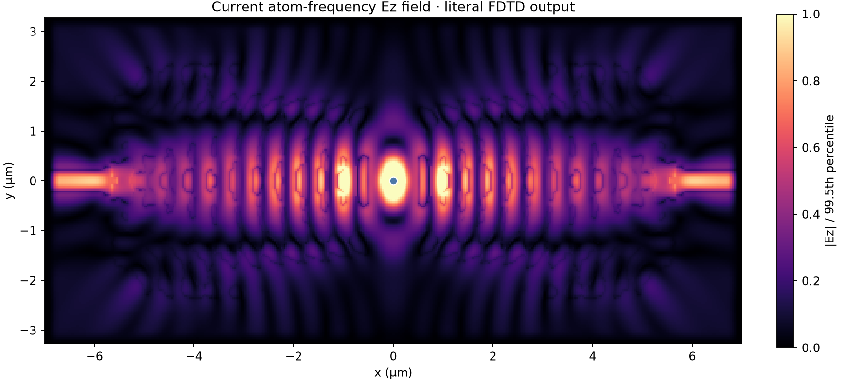
Warm-started 12-front cavity preserved after 795 LDOS updates and 294 bounded-beta updates.
Curved mirrors · 8 / 12 / 16 fronts
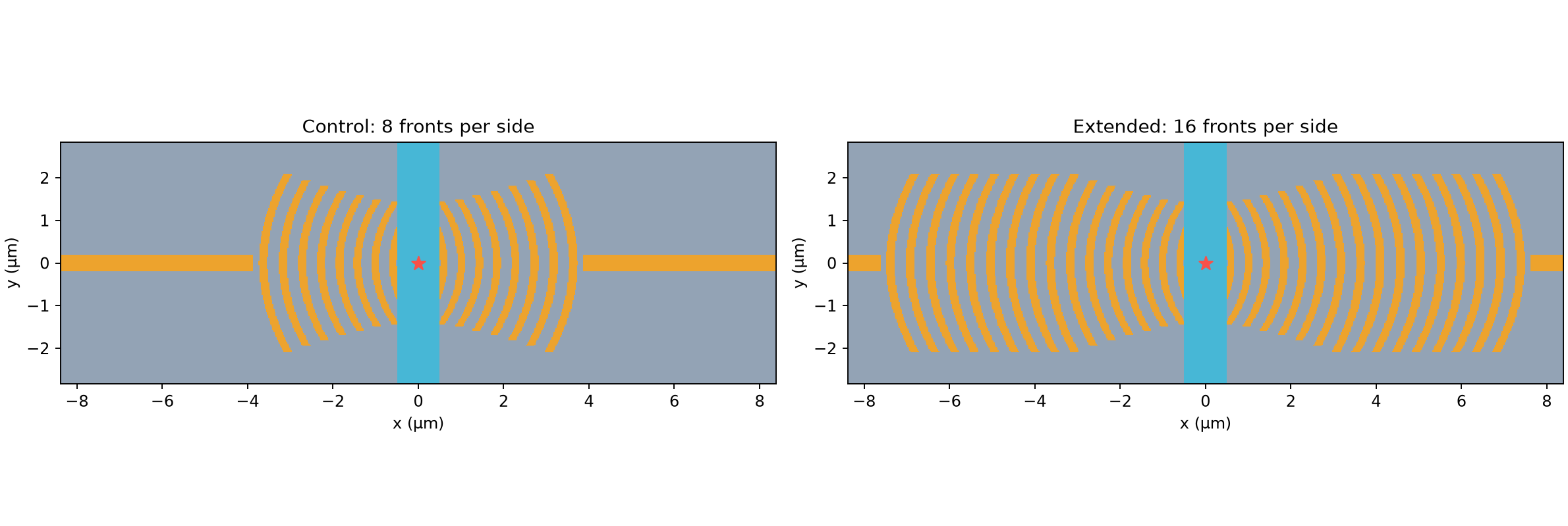
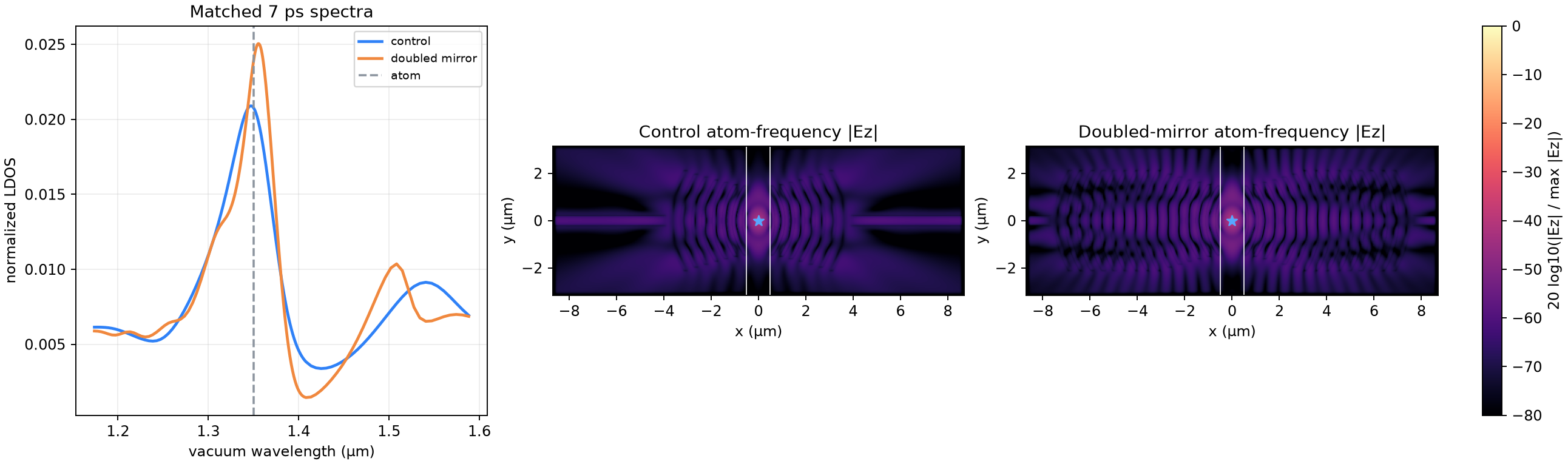
Controlled mirror-count comparison at fixed transverse domain size, including the 12-front seed used downstream.
Facing curved mirrors · parameterization
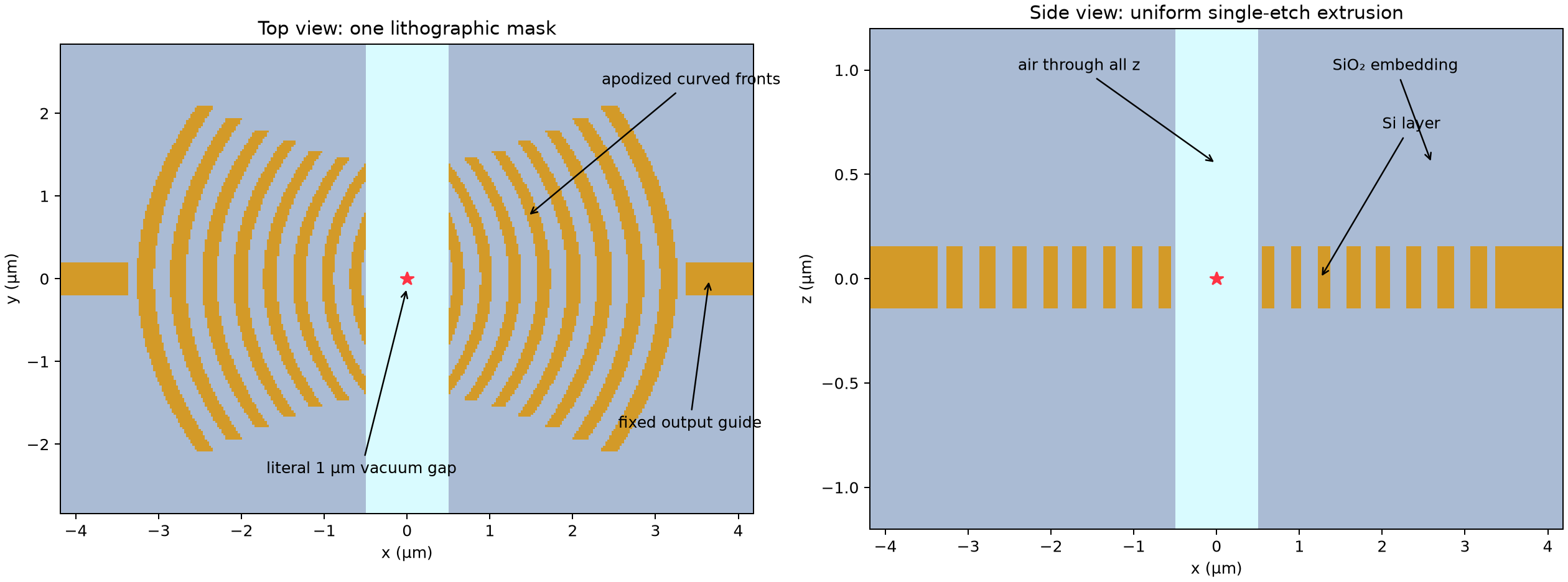
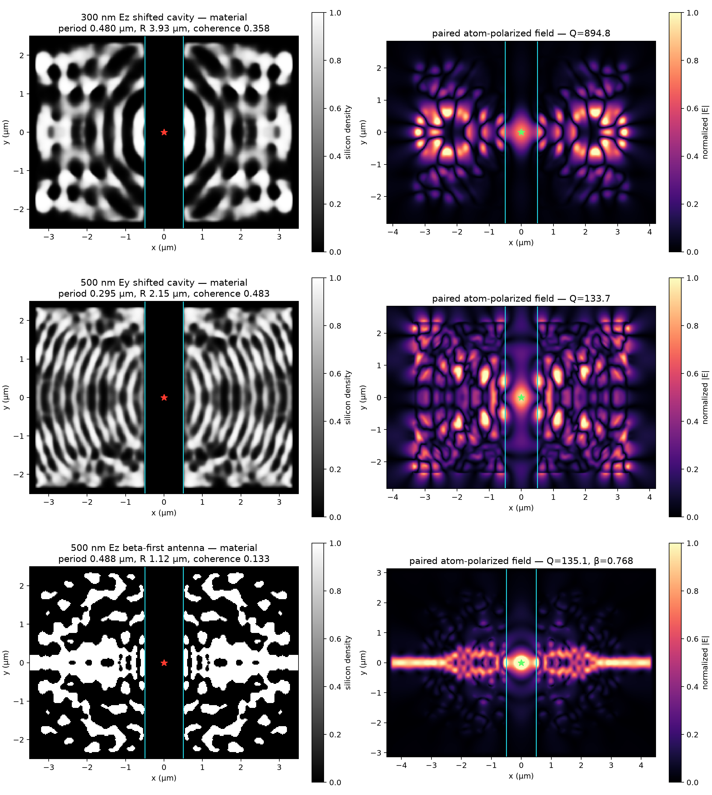
The geometry model distilled from the most promising intermediate structures: spacing, curvature, apodization, thickness, and embedding.
Curved mirrors · 12-hour parameter sweep
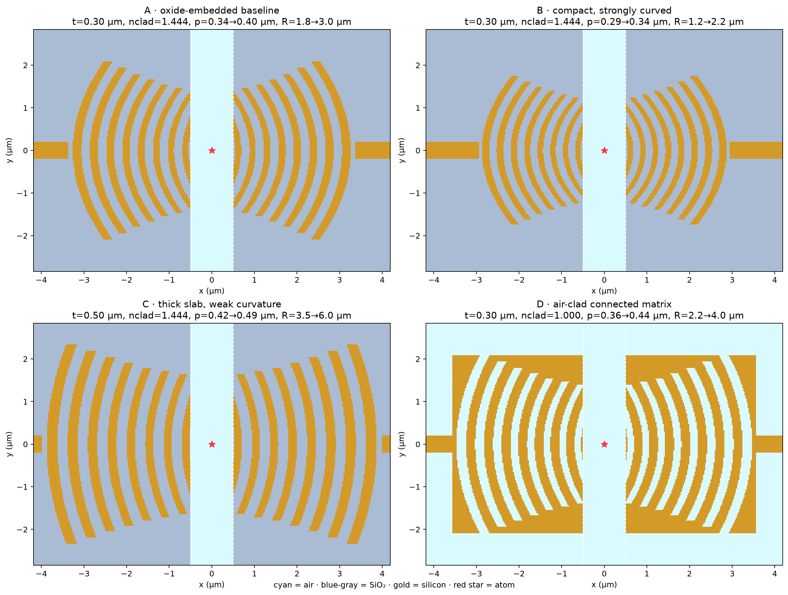
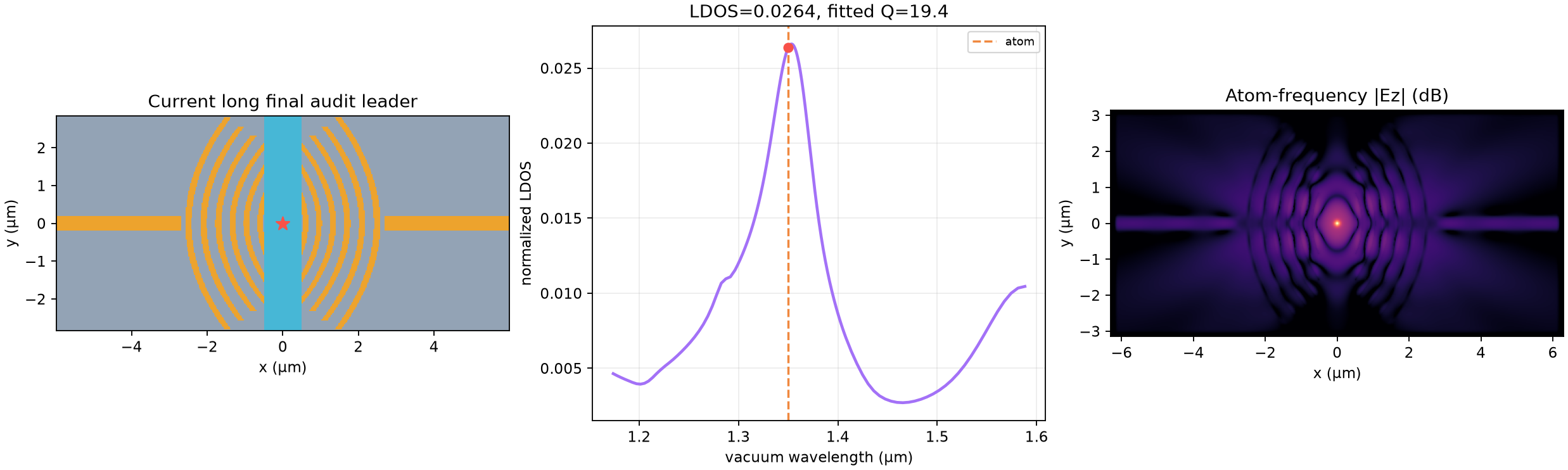
The broad thickness, gap, mirror-spacing, apodization, segment-count, and SiO₂-embedding screen that selected the optimization seed.
Axisymmetric atom hole · radial Q/V
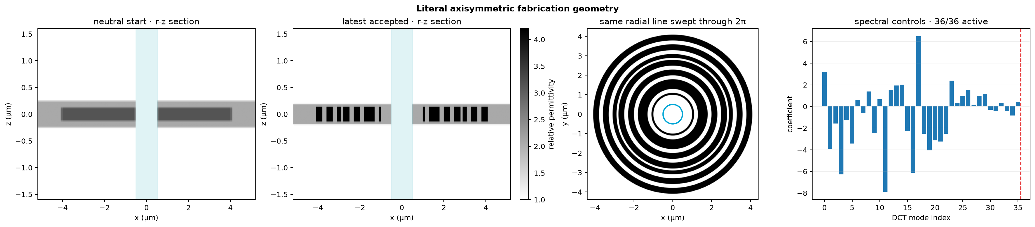
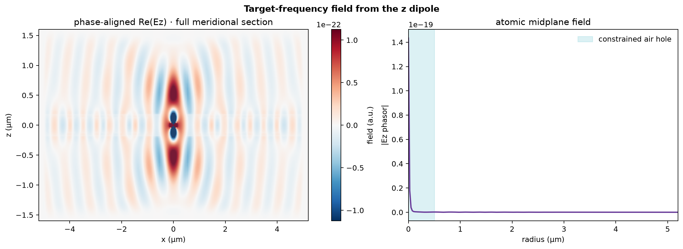
One-dimensional cosine controls revolved through 2π, with Cartesian audits exposing the reduced-model discrepancy.
Square atom hole · waveguide beta
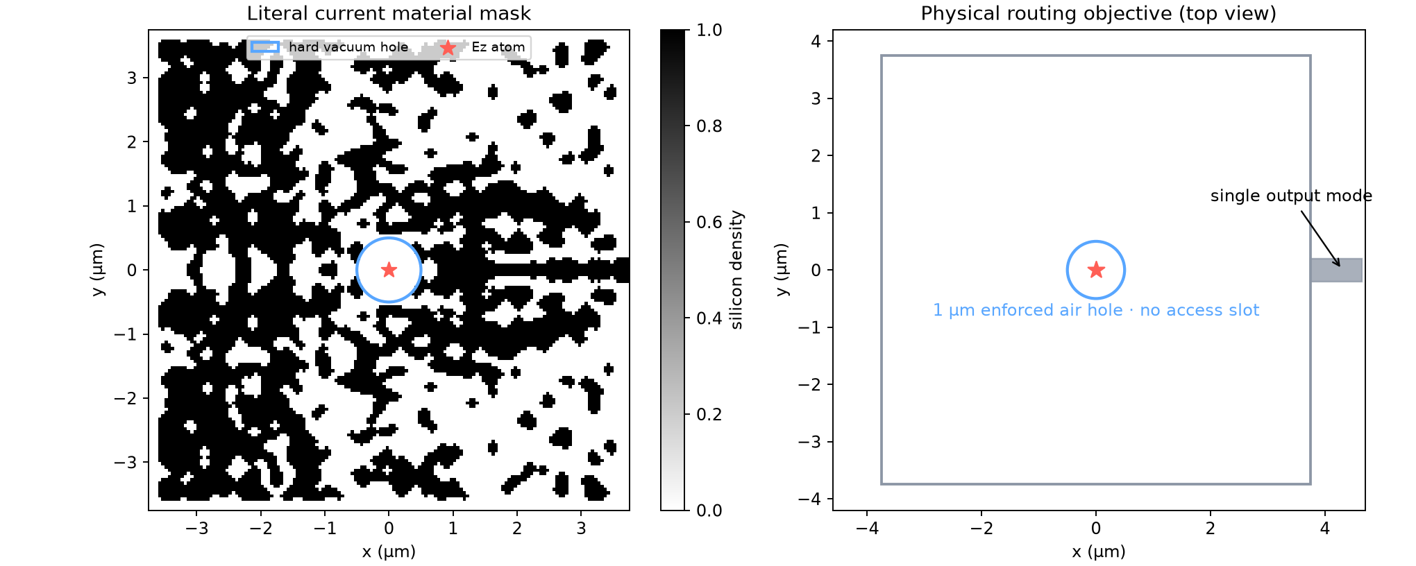
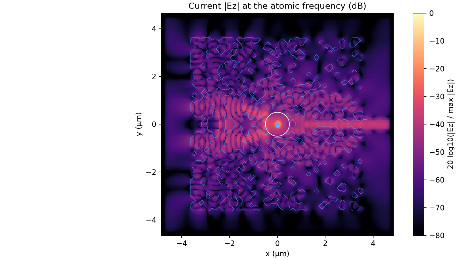
7.5 µm no-slot beta-first campaign with a protected central hole, attached guide, and pole surveillance.
From-scratch atom coupler · beta first
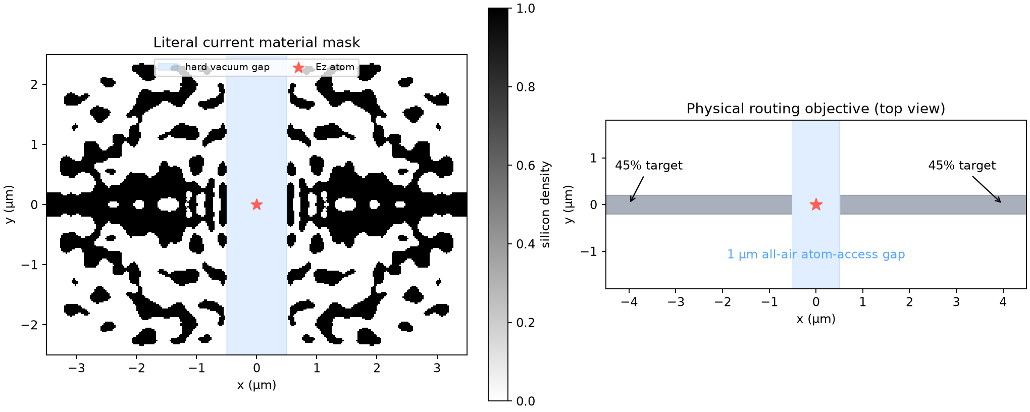
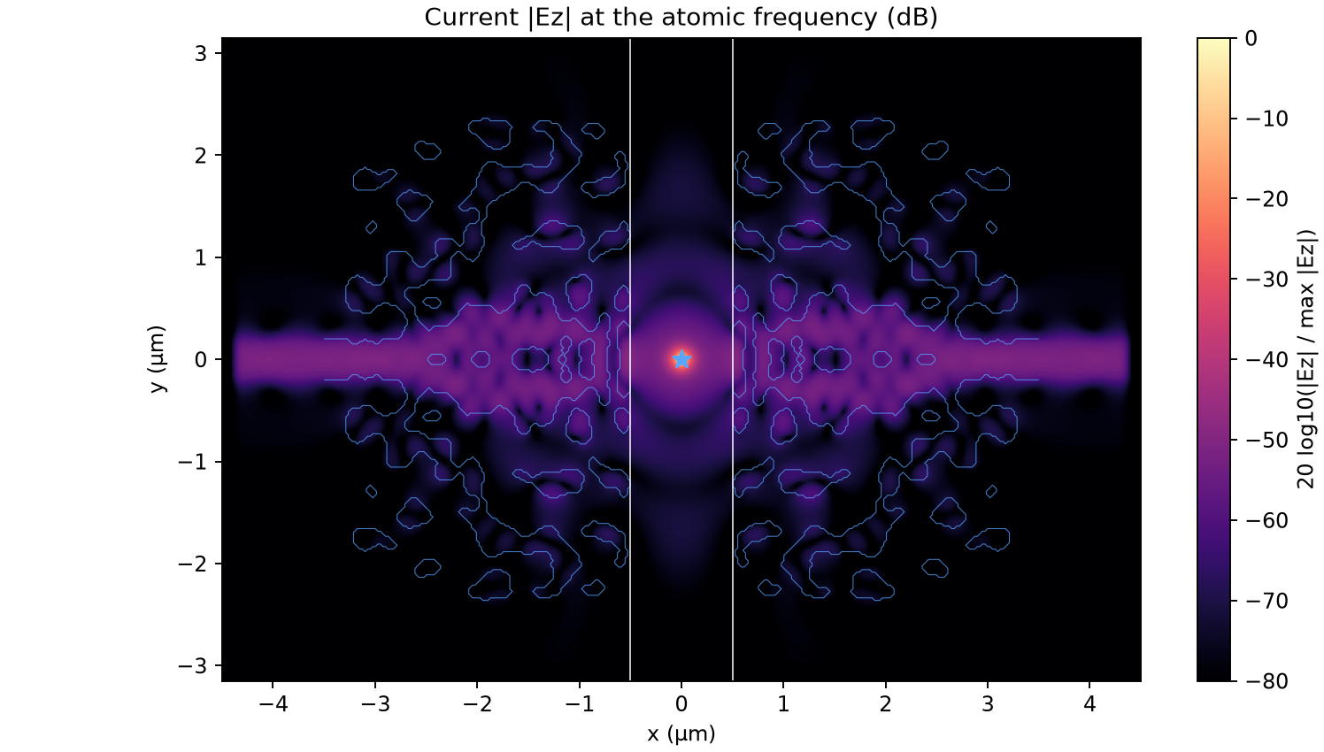
Single-etch atom-to-waveguide topology discovery, guided branching-ratio objective, and shifted-pole continuation.
Atom coupler · beta sign-off
The independent spectrum, branching-ratio, hard-mask, and density checks applied to the beta-first final checkpoint.
From-scratch atom cavity · LDOS first
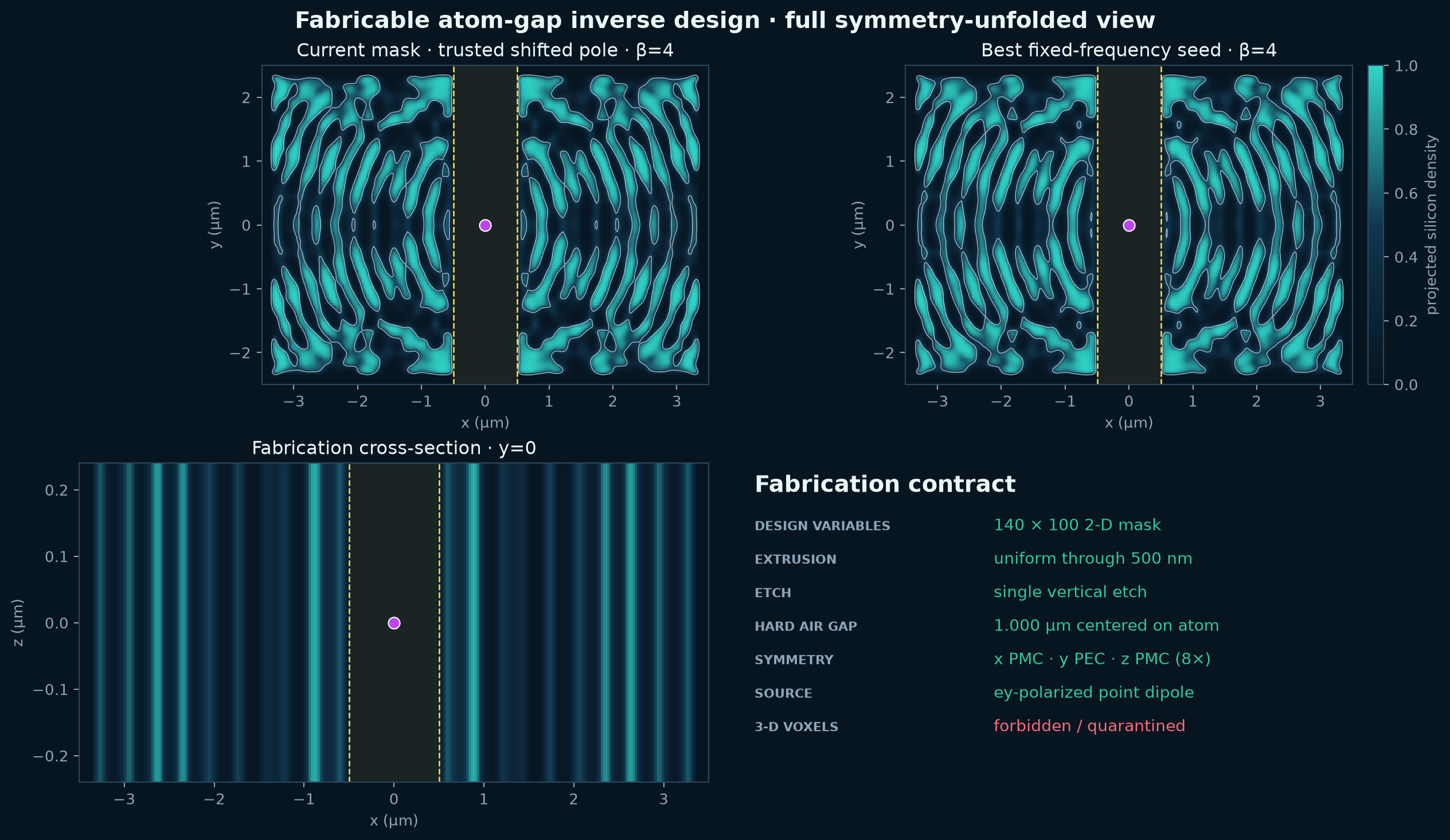
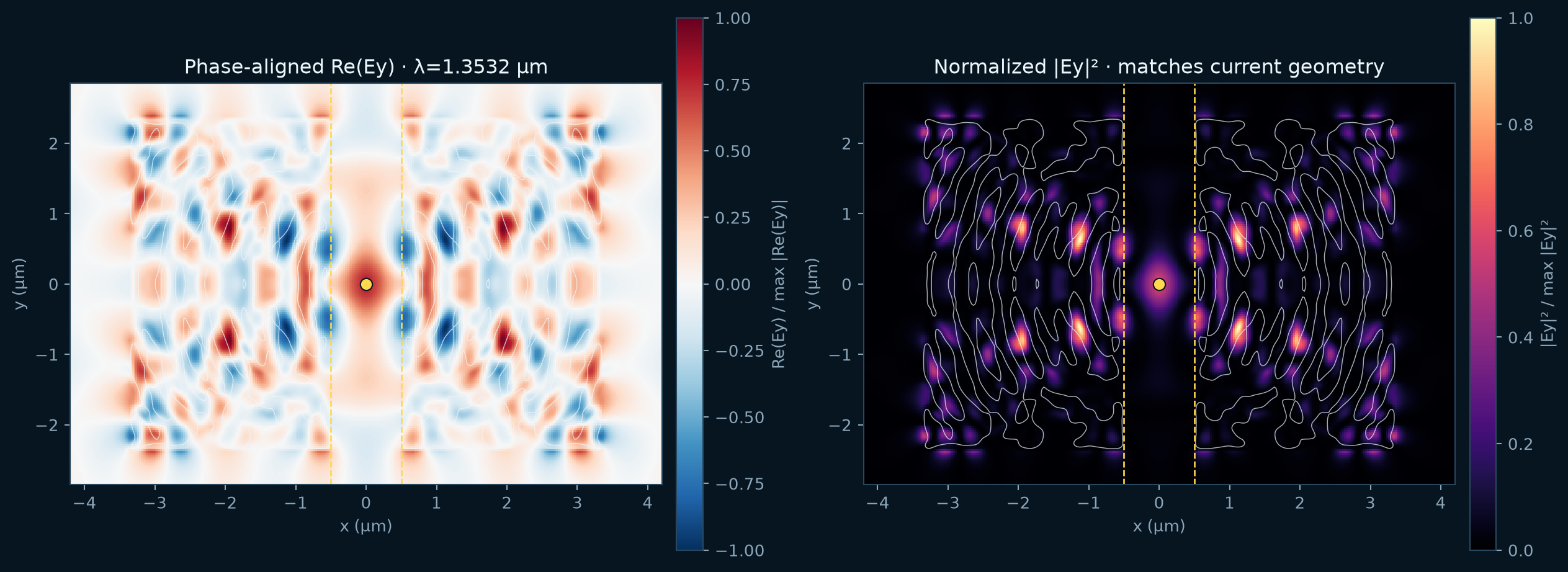
Historical free-form LDOS campaign whose nearly static gray-material stage motivated stronger continuation controls.
One-micron atom gap cavity
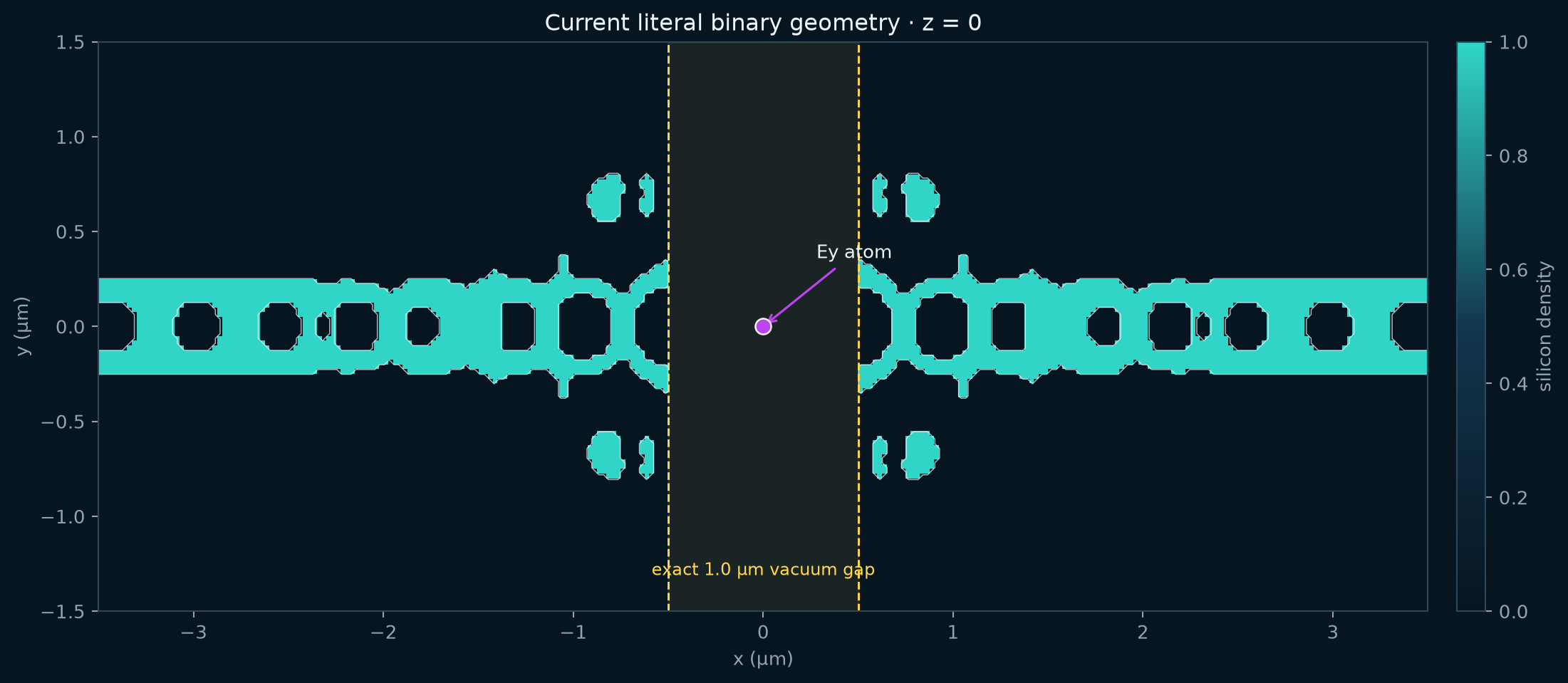
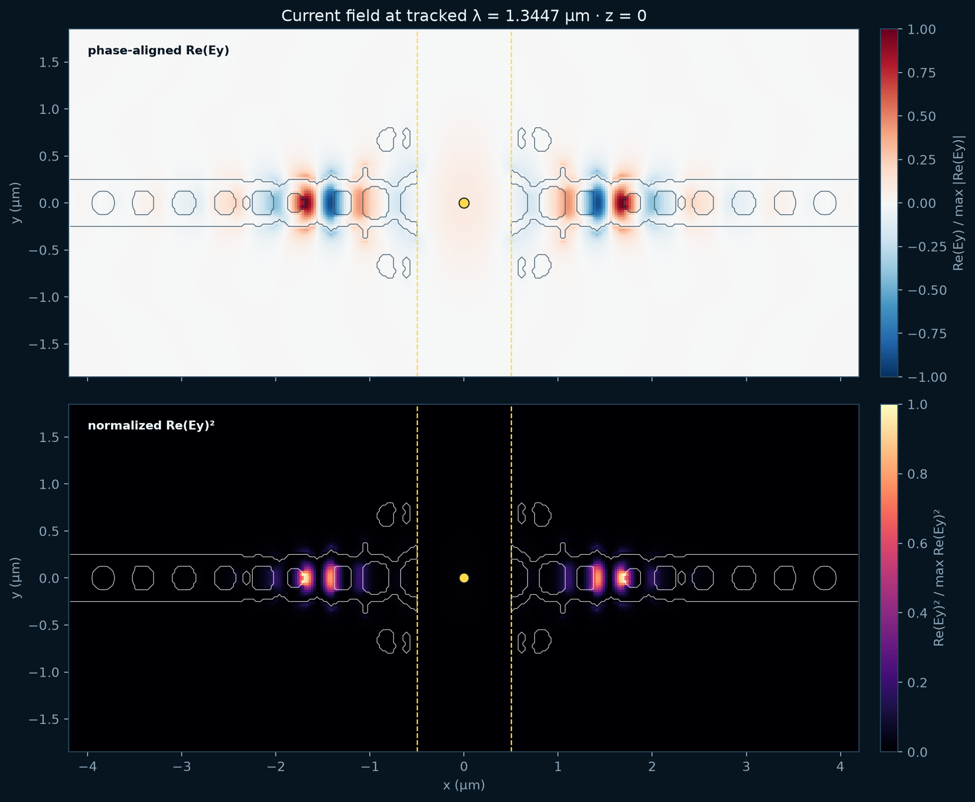
The original hard-gap free-form campaign, retained with its literal geometry and evidence that the mode remained dielectric-centered.
Atom gap · Q and Purcell sign-off
The fail-closed replay requirements for claiming Q≥1,000 and Purcell≥5 in the one-micron dielectric gap.
Folded SiN cavity · atom-to-waveguide
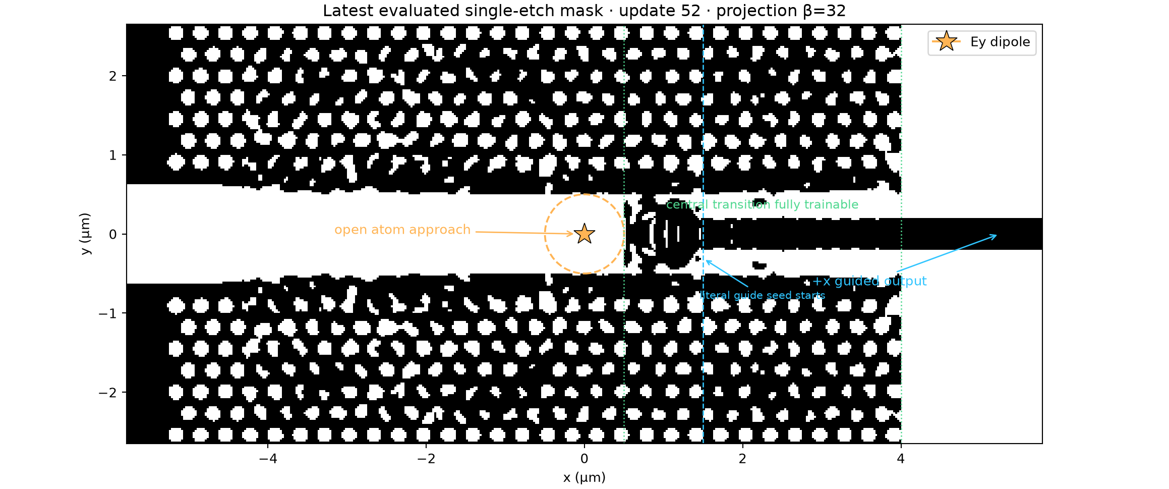
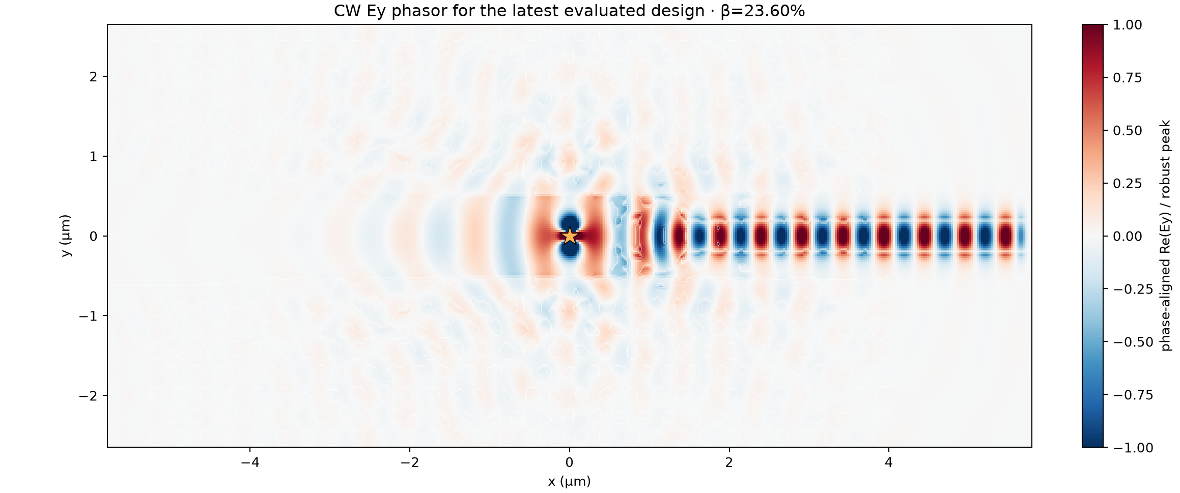
Opposed 780 nm quasi-2D cavities with the exit guide inside the design region and directional-loss telemetry.
SiN atom slot · perpetual beta campaign
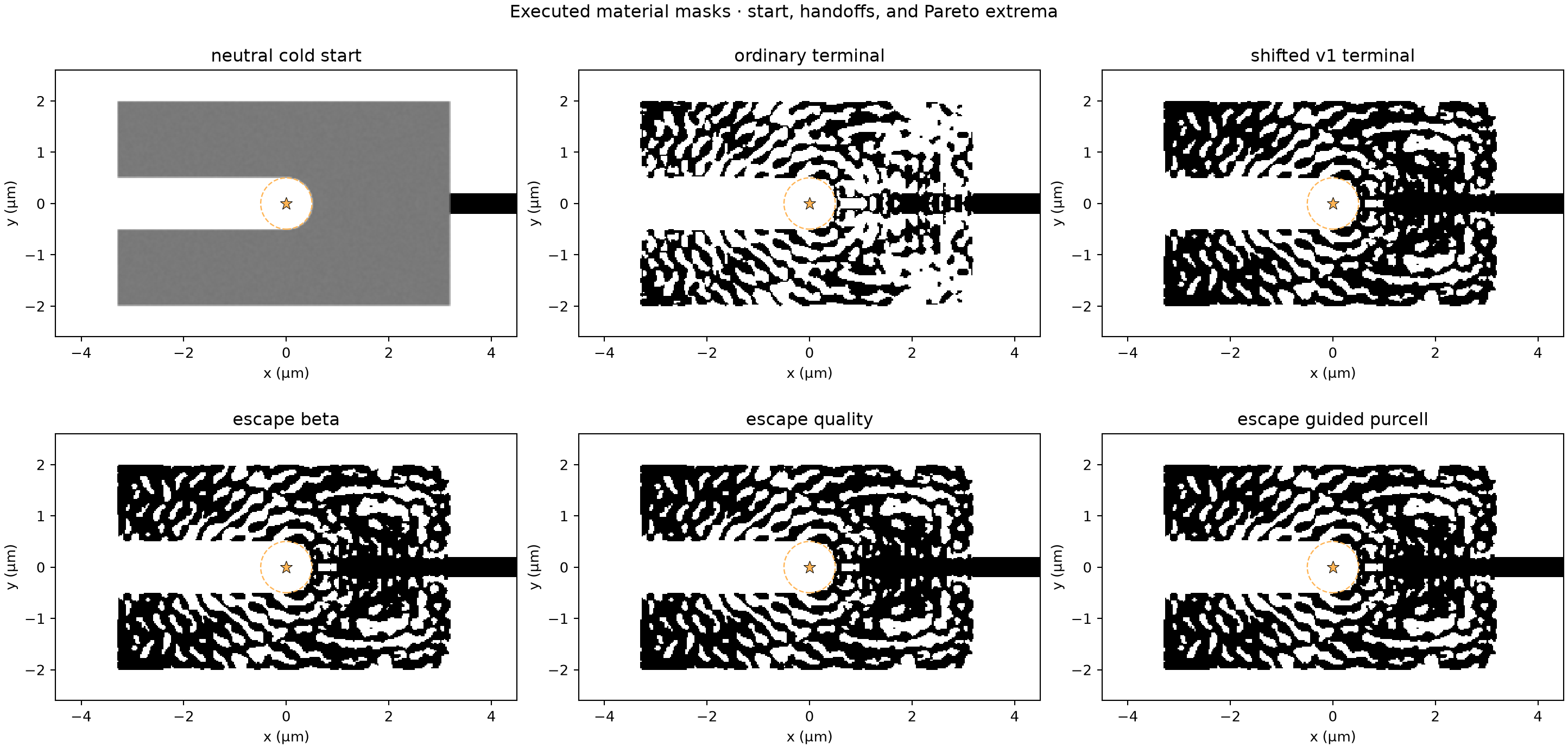
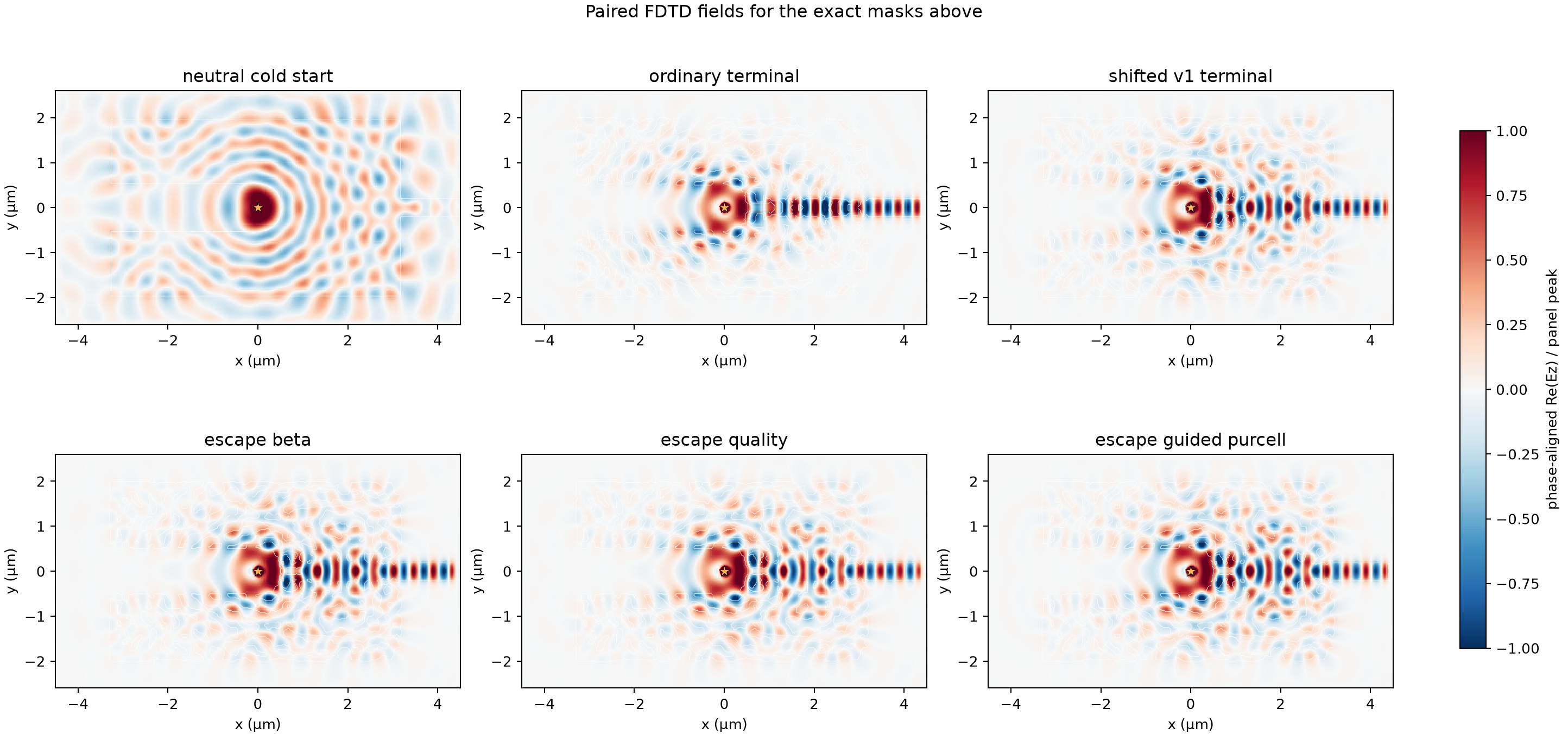
The complete multi-stage beta campaign: accepted methods, rejected branches, Pareto checkpoints, and terminal morphology failure.
SiN atom slot · compact checkpoint
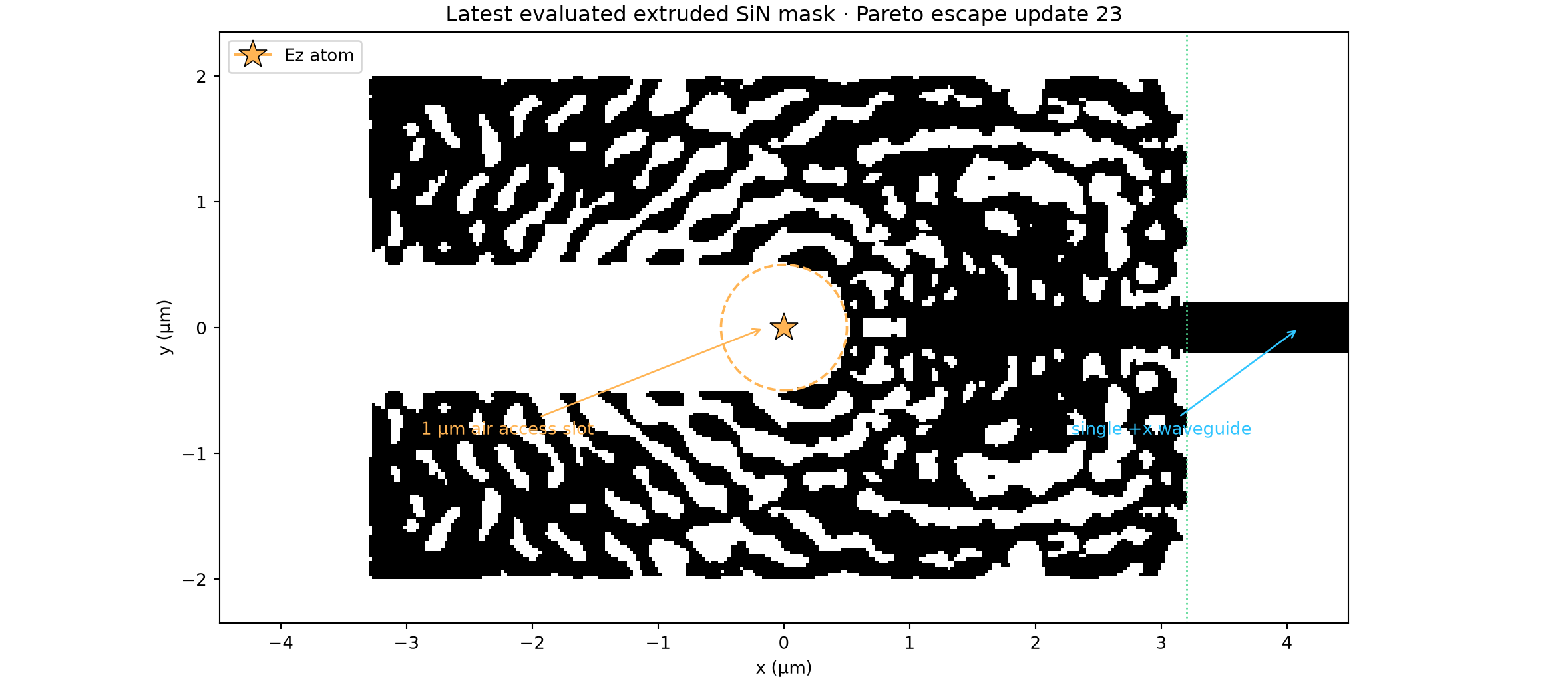
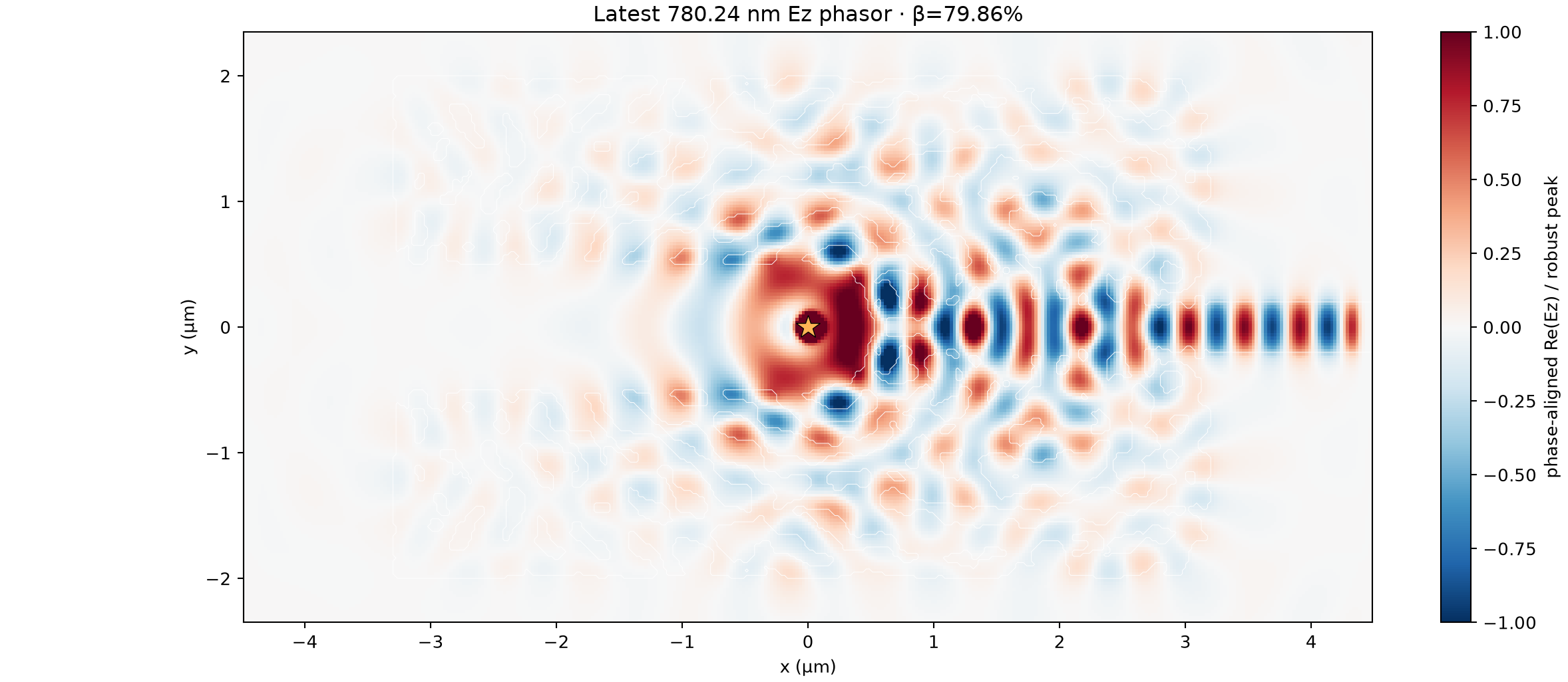
The last literal mask, field, guided channels, loss directions, pole, and shifted-beta metrics from the stopped campaign.
Zhang-style quasi-2D cavity · remote atom
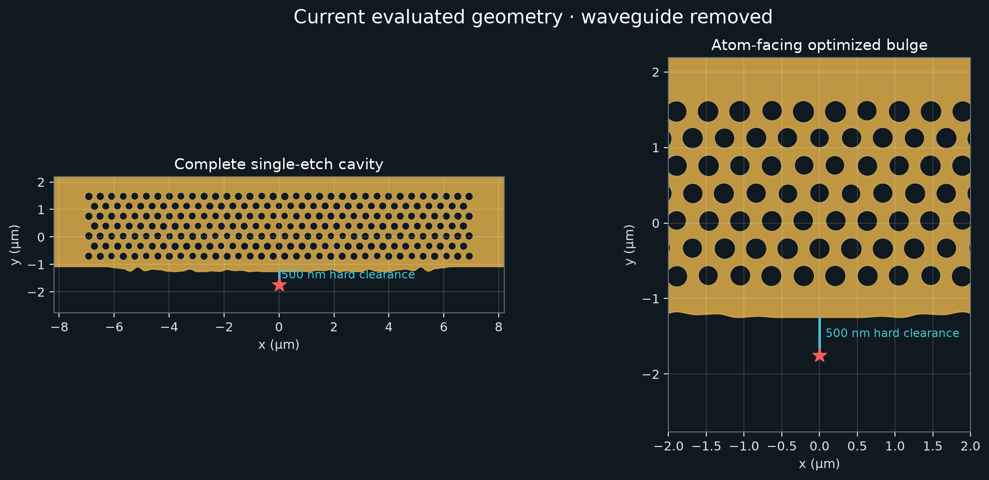
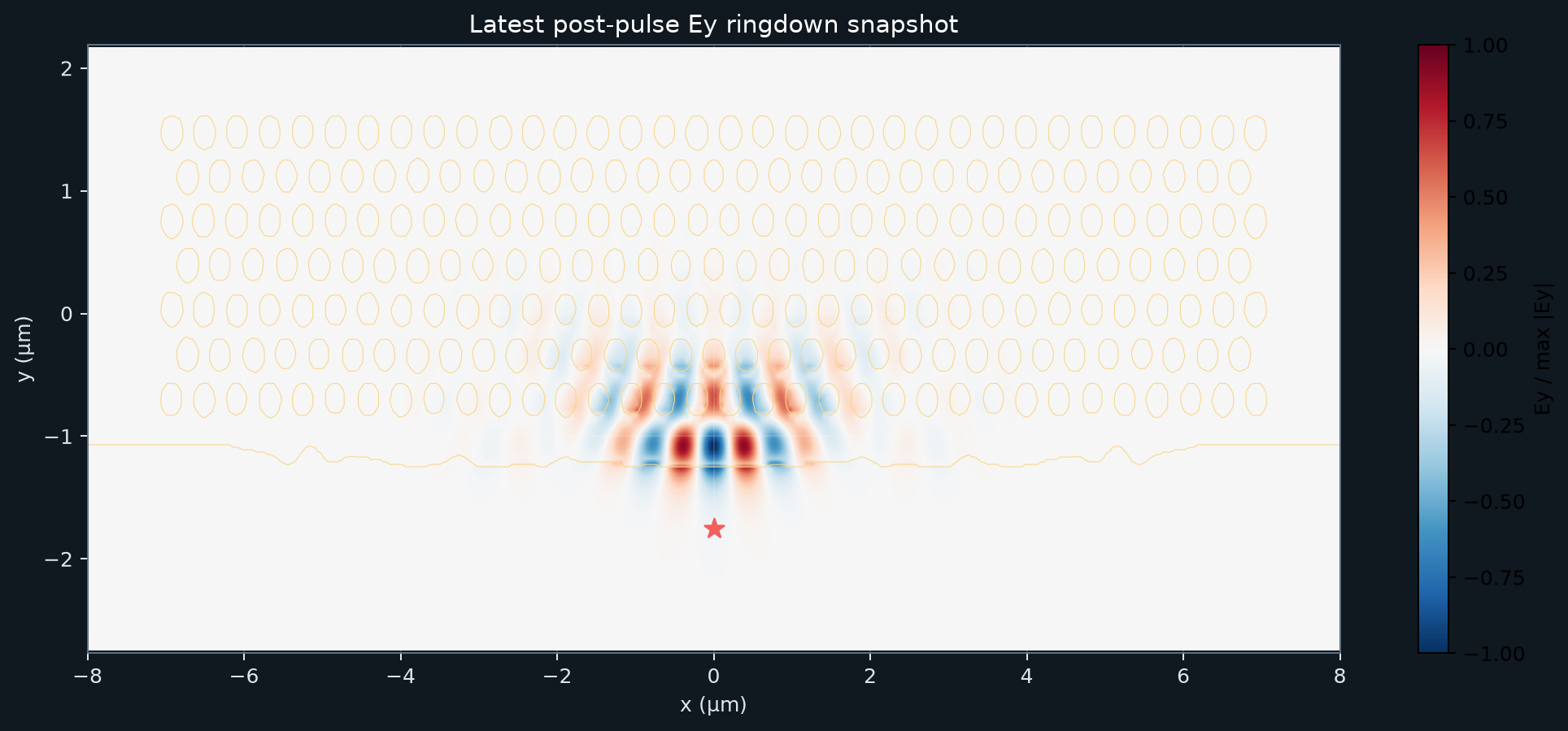
Parametric bulge and movable-hole optimization for an atom constrained 0.5 µm from the silicon device edge.
Zhang-style cavity · unloaded baseline
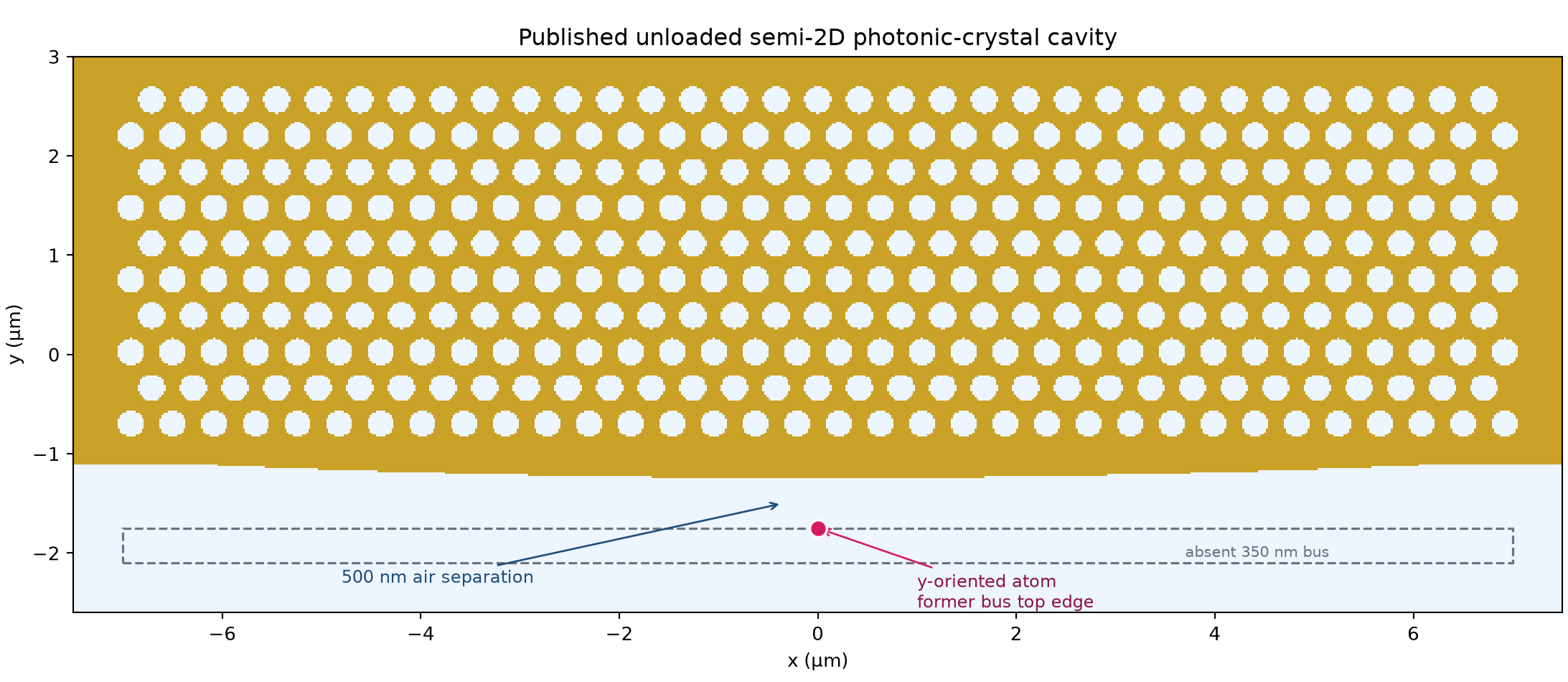
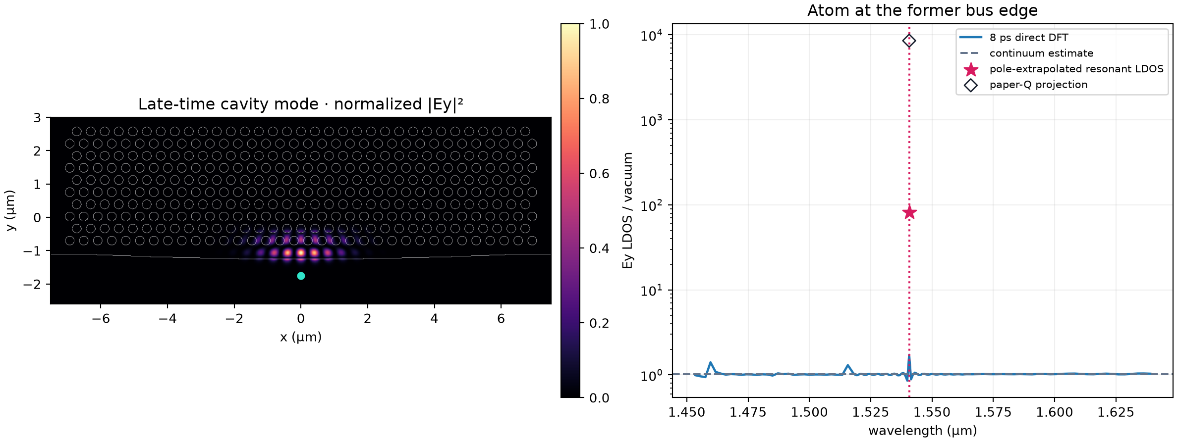
The full paper cavity without its bus waveguide, including the pole and atom LDOS 0.5 µm from the dielectric edge.
780 nm SiN quasi-2D cavity
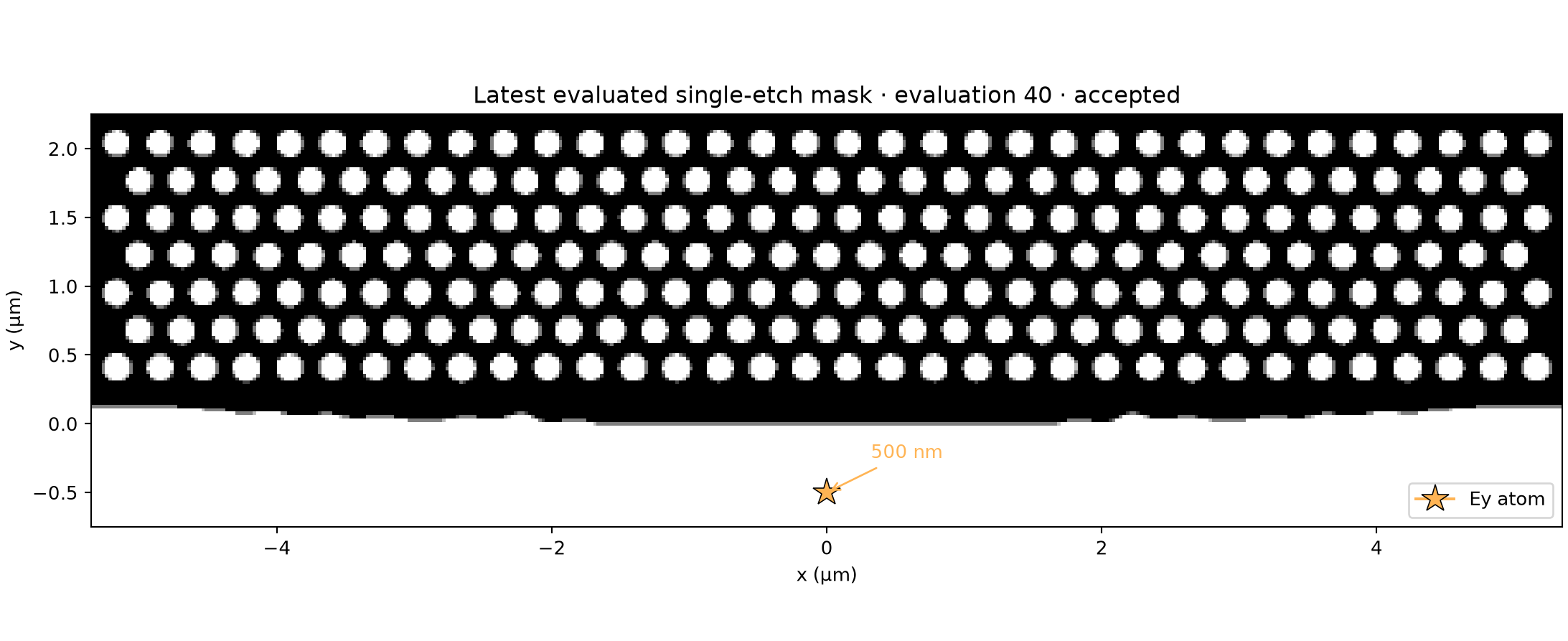
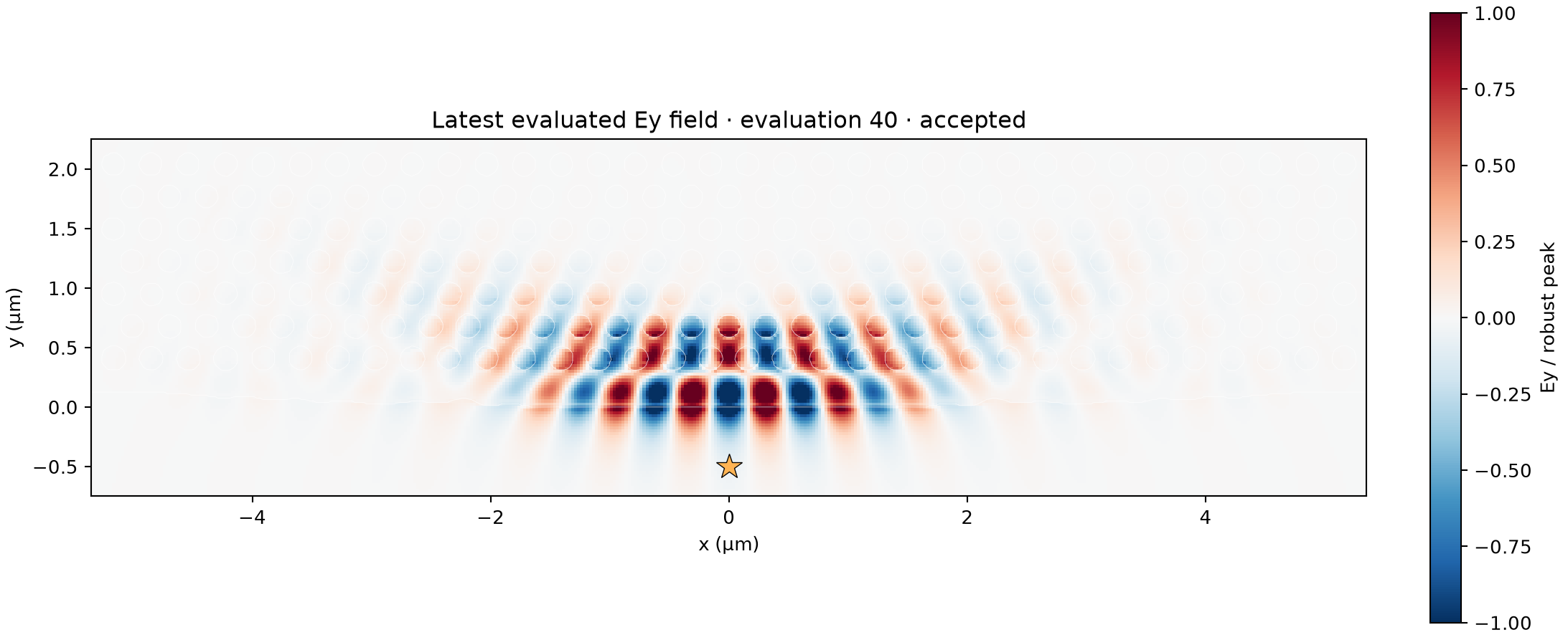
Material-scaled remote-atom campaign targeting a 780.24 nm resonance and enhanced evanescent coupling.
Ez bandgap · quasi-2D atom interface
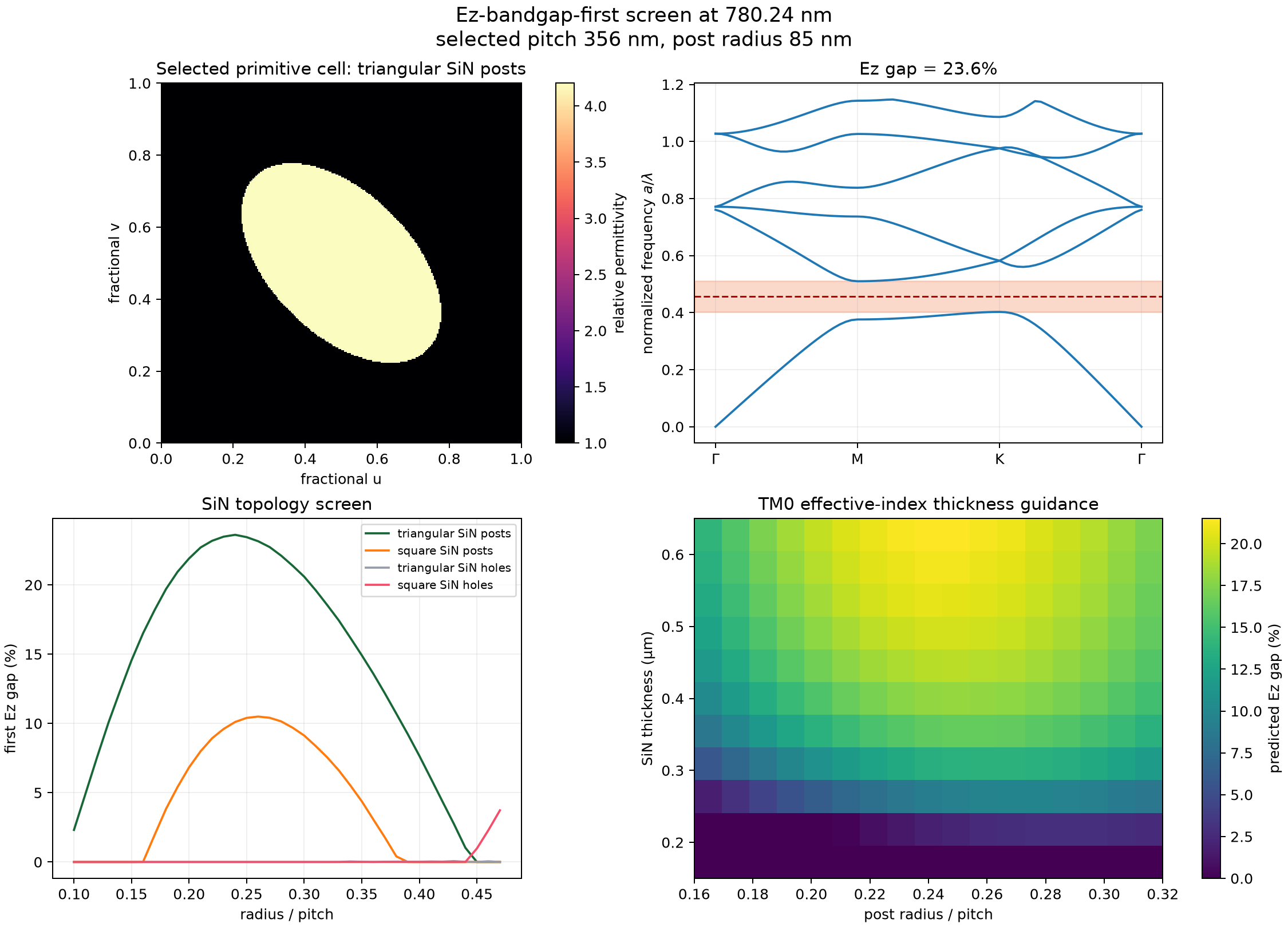
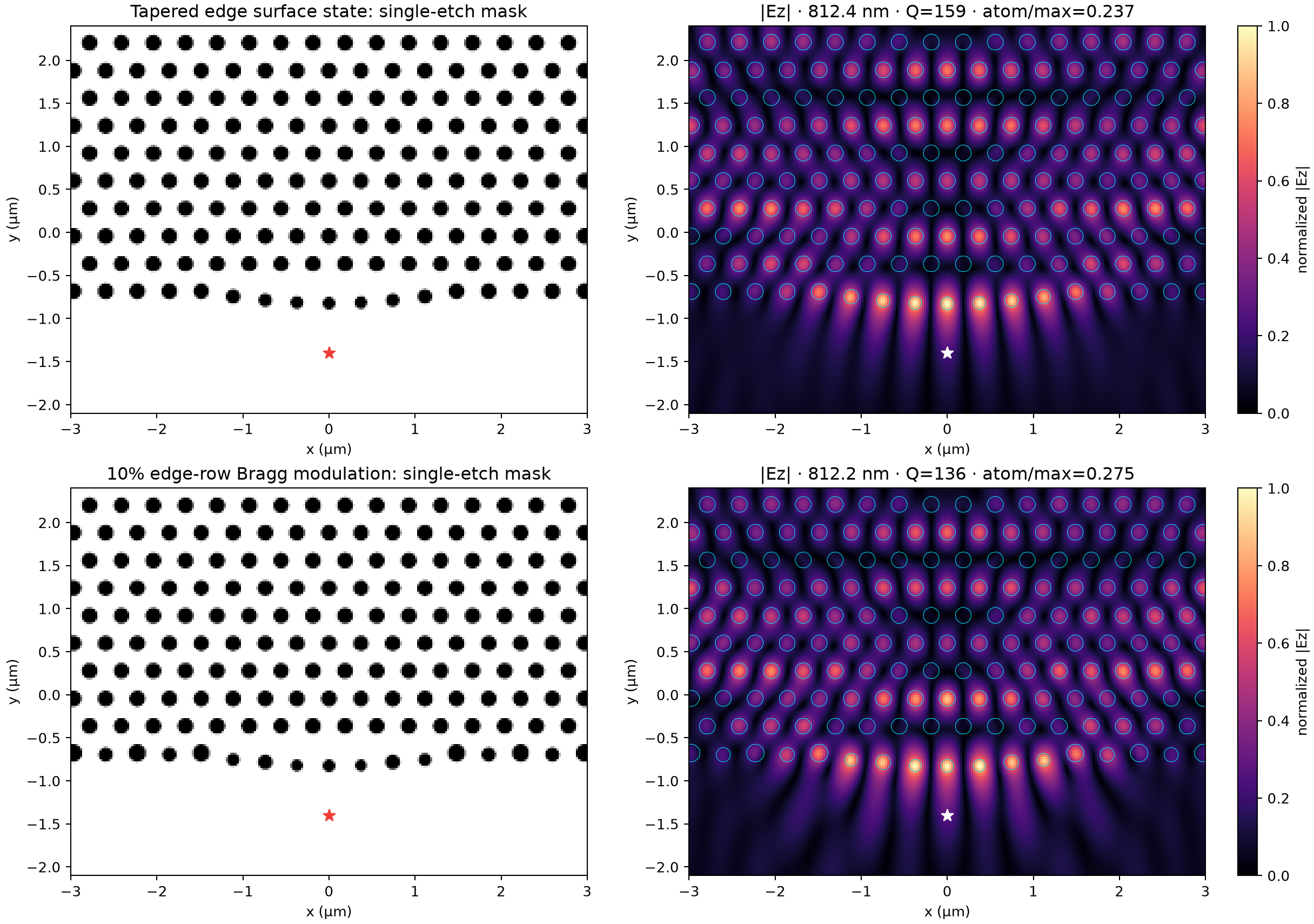
Fabricability-aware slab-hole/post screen and edge taper built to couple a z-oriented atom to a quasi-2D mode.