Integrated photonics#
The guided-wave workflow begins with a cross-sectional mode, then adds calibrated ports and progressively more sensitive geometry.
1. Solve the guide mode#
uv run fdtdx-bench run --case analytical_mode_waveguide
This checks silicon-slab effective index and confinement. Visualize the transverse eigenfield and verify its parity before using it as a source.
2. Calibrate a straight port#
uv run fdtdx-bench run --case analytical_waveguide_sparams
uv run fdtdx-bench run --case parity_waveguide_TE
The Tidy3D-backed straight guide records transmitted power 1.000053 against 1.000000. This near-unity control is essential: without it, device loss and port-normalization error cannot be separated.
3. Split power#
uv run fdtdx-bench run --case parity_y_junction
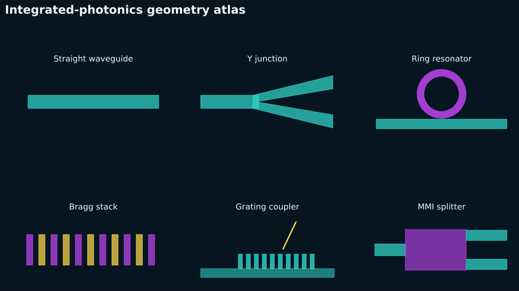
The coarse Y junction records output powers 0.203 and 0.262, sum 0.465, against Tidy3D’s 0.270, 0.270, sum 0.541. Each metric stays within its declared resolution-aware budget. The asymmetry is a warning that this grid is suitable for capability validation, not precision splitter design.
4. Add spectral structure#
uv run fdtdx-bench run --case parity_bragg_stack
uv run fdtdx-bench run --case parity_ring_bus
The bus-coupled ring uses fill-fraction subpixel smoothing and records 0.0254 relative-\(L_2\) spectral error. Its resolution factor is 0.8, so the case explicitly scales its tolerance. It validates mode-coupled resonator behavior, not a converged high-\(Q\) linewidth.
5. Move to complete devices#
The real-world ladder adds ten forward simulations sourced from official Tidy3D notebooks:
uv run fdtdx-bench run --case device_directional_coupler
uv run fdtdx-bench run --case device_waveguide_crossing
uv run fdtdx-bench run --case device_euler_bend
uv run fdtdx-bench run --case device_edge_coupler
uv run fdtdx-bench run --case device_mmi_1x4
uv run fdtdx-bench run --case device_bragg_grating
uv run fdtdx-bench run --case device_nanobeam_cavity
uv run fdtdx-bench run --case device_polarization_splitter_rotator
The metasurface absorber and metalens extend the same workflow beyond guided-wave PICs. See the illustrated 15-device walkthrough for geometry, field schematics, spectra, scalar observables, and inverse-designed material maps.
The device cases intentionally share mesh selection, connected-geometry rasterization, incident calibration, modal overlap, and energy-decay termination. When a new device requires many private resolution or normalization constants, treat that as evidence of missing automatic machinery rather than normal setup.
Current frontier#
Three older references remain blocked with recorded reasons: a ring-drop spectrum, a grating-coupler spectrum, and an early MMI reference that was not reproducible. The newer official-notebook 1×4 MMI is a distinct, trusted case and passes. Keeping the quarantined artifacts visible prevents a newer success from rewriting the history of an unreliable comparison.