Waveguide crossing: transmission and crosstalk#
Orthogonal convex-cosine tapers form a compact O-band crossing with a through port and an explicit crosstalk port.
This executable notebook follows the same progression as the official Tidy3D example: inspect parameters, construct geometry and ports, plot the actual voxelized scene, execute one broadband FDTDX simulation, visualize the recorded electric field, and compare the reduced observables with a frozen Tidy3D result.
Imports and accelerator#
import os
os.environ.setdefault("XLA_PYTHON_CLIENT_PREALLOCATE", "false")

from time import perf_counter
import warnings
import matplotlib.pyplot as plt
import numpy as np
import pandas as pd
import jax
import fdtdx
from IPython import get_ipython

from benchmarks.device_specs import MODE_PORT_SPECS

get_ipython().run_line_magic("matplotlib", "inline")
warnings.filterwarnings("ignore", category=FutureWarning, module=r"tidy3d\.components\.mode")
plt.rcParams.update({"figure.figsize": (9, 4.5), "figure.dpi": 120})
CASE_ID = "device_waveguide_crossing"
UM = 1e-6
spec = MODE_PORT_SPECS[CASE_ID]
print(f"JAX devices: {jax.devices()}")
JAX devices: [CudaDevice(id=0)]
1. Physical and numerical parameters#
parameters = pd.Series(
    {
        "domain (µm)": spec.domain_um,
        "center wavelength (µm)": spec.wavelength0_um,
        "monitor wavelengths (µm)": spec.wavelengths_um,
        "grid pitch (µm)": spec.dl_um,
        "maximum run time (ps)": spec.run_time_s * 1e12,
        "background index": spec.background_index,
        "device thickness (µm)": spec.thickness_um,
        "PML cells per face": spec.pml_layers,
    },
    name="value",
)
display(parameters.to_frame())
print(spec.adaptation)
| value | |
|---|---|
| domain (µm) | (9.0, 9.0, 1.2) |
| center wavelength (µm) | 1.31 |
| monitor wavelengths (µm) | (1.26, 1.31, 1.36) |
| grid pitch (µm) | 0.025 |
| maximum run time (ps) | 1.5 |
| background index | 1.444 |
| device thickness (µm) | 0.161 |
| PML cells per face | 8 |
Official convex-cosine crossing shortened from 5.3 to 4.0 um per taper; same O-band ports.
2. Geometry and ports#
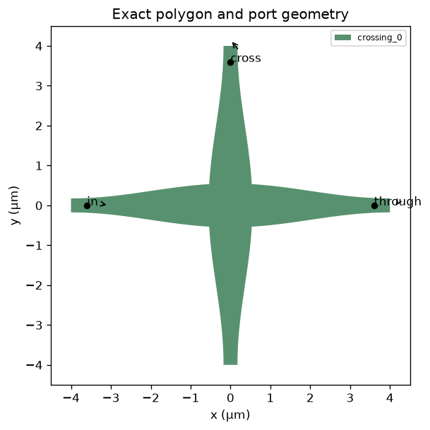
The plotted vertices below are the arrays passed to fdtdx.ExtrudedPolygon.
Port arrows use the same centers and propagation directions passed to the source
and mode-overlap detectors.
fig, ax = plt.subplots(figsize=(11, 5.5))
for layer in spec.layers:
    vertices = np.asarray(layer.vertices_um)
    ax.fill(vertices[:, 0], vertices[:, 1], alpha=0.72, label=layer.name)

ports = (spec.input_port, *spec.output_ports)
for port in ports:
    x, y, _ = port.center_um
    delta = 0.55 if port.direction == "+" else -0.55
    dx, dy = (delta, 0) if port.axis == 0 else (0, delta)
    ax.annotate(port.name, (x + dx, y + dy), (x, y), arrowprops={"arrowstyle": "->"})
    ax.scatter([x], [y], s=22, color="black")

ax.set(
    xlabel="x (µm)", ylabel="y (µm)", title="Exact polygon and port geometry",
    xlim=(-spec.domain_um[0] / 2, spec.domain_um[0] / 2),
    ylim=(-spec.domain_um[1] / 2, spec.domain_um[1] / 2),
    aspect="equal",
)
ax.legend(loc="best", fontsize=7)
plt.show()
3. Build the FDTDX scene#
Geometry is extruded through the device layer. PortSpec selects either a solved
waveguide mode or an analytic Gaussian source. The optional FieldMonitorSpec
records a complex electric-field phasor across the device plane during the same
pulsed run used for S-parameters.
domain_m = tuple(value * UM for value in spec.domain_um)
resolution = spec.dl_um * UM
materials = {}
polygons = []
for layer in spec.layers:
    vertices = np.asarray(layer.vertices_um) * UM
    center = 0.5 * (vertices.min(axis=0) + vertices.max(axis=0))
    material = materials.setdefault(
        layer.refractive_index,
        fdtdx.Material(permittivity=layer.refractive_index**2),
    )
    polygon = fdtdx.ExtrudedPolygon(
        name=layer.name,
        vertices=vertices - center,
        axis=2,
        partial_real_shape=(None, None, spec.thickness_um * UM),
        materials={"device": material},
        material_name="device",
        placement_order=layer.placement_order,
        subpixel_smoothing=True,
    )
    polygons.append((polygon, (center[0] + domain_m[0] / 2, center[1] + domain_m[1] / 2, domain_m[2] / 2)))

def make_port(port):
    center = tuple((coordinate + extent / 2) * UM for coordinate, extent in zip(port.center_um, spec.domain_um, strict=True))
    return fdtdx.PortSpec(
        center=center, axis=port.axis, direction=port.direction,
        width=port.width_um * UM, height=port.height_um * UM,
        mode_index=0, filter_pol=port.filter_pol,
        source_kind=port.source_kind,
        gaussian_mode_radius=(port.gaussian_mode_radius_um * UM if port.gaussian_mode_radius_um else None),
        name=port.name,
    )

field_monitor = fdtdx.FieldMonitorSpec(
    name="field_xy",
    center=(domain_m[0] / 2, domain_m[1] / 2, domain_m[2] / 2),
    size=(domain_m[0], domain_m[1], resolution),
    wavelengths=(spec.wavelength0_um * UM,),
    components=("Ex", "Ey", "Ez"),
)
objects, arrays, config = fdtdx.setup_sparams_simulation(
    polygons=polygons,
    input_ports=[make_port(spec.input_port)],
    output_ports=[make_port(port) for port in spec.output_ports],
    wavelength=spec.wavelength0_um * UM,
    wavelengths=tuple(value * UM for value in spec.wavelengths_um),
    resolution=resolution,
    max_time=spec.run_time_s,
    domain_size=domain_m,
    background_material=fdtdx.Material(permittivity=spec.background_index**2),
    pml_layers=spec.pml_layers,
    field_monitors=(field_monitor,),
)
print(f"Yee grid: {objects.volume.grid_shape}")
print(f"Time-step ceiling: {config.time_steps_total:,}")
Yee grid: (376, 376, 64)
Time-step ceiling: 31,470
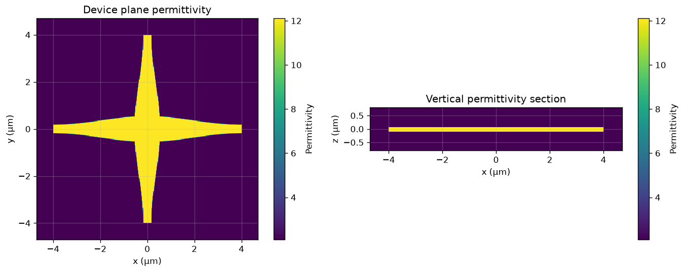
4. Plot the voxelized simulation geometry#
fig, axes = plt.subplots(1, 2, figsize=(12, 4.5))
fdtdx.plot_material_from_side(config, arrays, "z", position=0.0, ax=axes[0], plot_legend=True)
fdtdx.plot_material_from_side(config, arrays, "y", position=0.0, ax=axes[1], plot_legend=True)
axes[0].set_title("Device plane permittivity")
axes[1].set_title("Vertical permittivity section")
plt.tight_layout()
plt.show()
5. Run one broadband simulation#
The mode source, normalization monitor, all output monitors, energy-decay monitor, and spatial field monitor are evaluated together. The simulation may terminate before the time ceiling once residual energy has decayed sufficiently.
started = perf_counter()
sparams, detector_states = fdtdx.calculate_sparam(
    objects, arrays, config, spec.input_port.name, show_progress=False,
)
elapsed_s = perf_counter() - started
print(f"Local FDTDX runtime: {elapsed_s:.1f} s")
Local FDTDX runtime: 57.1 s
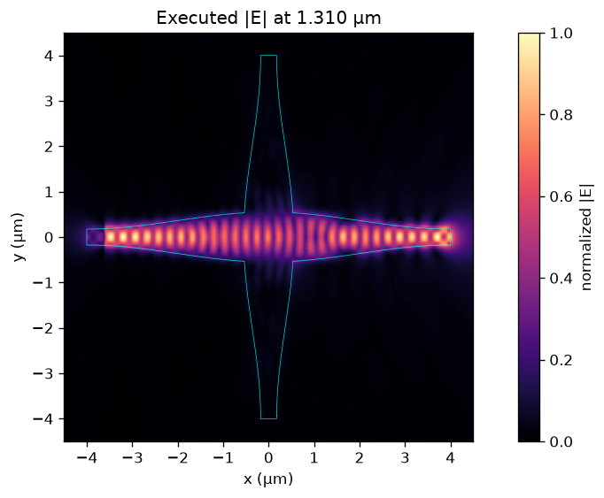
6. Plot the simulated electric field#
phasor = np.asarray(detector_states["field_xy"]["phasor"])[0, 0, :3]
field_magnitude = np.sqrt(np.sum(np.abs(phasor) ** 2, axis=0)).squeeze()
field_magnitude /= field_magnitude.max() + 1e-30
fig, ax = plt.subplots(figsize=(11, 5))
image = ax.imshow(
    field_magnitude.T, origin="lower",
    extent=(-spec.domain_um[0] / 2, spec.domain_um[0] / 2, -spec.domain_um[1] / 2, spec.domain_um[1] / 2),
    cmap="magma", vmin=0, vmax=1, aspect="equal",
)
for layer in spec.layers:
    vertices = np.asarray(layer.vertices_um)
    ax.plot(*np.vstack((vertices, vertices[0])).T, color="cyan", lw=0.45, alpha=0.8)
ax.set(xlabel="x (µm)", ylabel="y (µm)", title=f"Executed |E| at {spec.wavelength0_um:.3f} µm")
fig.colorbar(image, ax=ax, label="normalized |E|")
plt.show()
7. Port analysis#
The useful checks are through transmission, orthogonal crosstalk, and total monitored power.
wavelengths_um = np.asarray(spec.wavelengths_um)
powers = {
    port.name: np.abs(np.asarray(sparams[(port.name, spec.input_port.name)]).squeeze()) ** 2
    for port in spec.output_ports
}
total = sum(powers.values(), start=np.zeros_like(wavelengths_um))
if len(powers) > 1:
    stack = np.stack(list(powers.values()))
    uniformity = np.std(stack, axis=0) / (np.mean(stack, axis=0) + 1e-30)

golden = np.load(f"benchmarks/goldens/{CASE_ID}.npz", allow_pickle=True)
colors = plt.cm.viridis(np.linspace(0.1, 0.9, len(powers)))
fig, ax = plt.subplots(figsize=(9, 4.8))
for (port_name, values), color in zip(powers.items(), colors, strict=True):
    ax.plot(wavelengths_um, values, "o-", color=color, label=f"FDTDX · {port_name}")
    ax.plot(wavelengths_um, golden[port_name], "x--", color=color, alpha=0.65, label=f"Tidy3D · {port_name}")
ax.set(xlabel="wavelength (µm)", ylabel="normalized modal power", title="Port spectra")
ax.grid(alpha=0.25)
ax.legend(ncol=2, fontsize=8)
plt.show()

table = pd.DataFrame({"wavelength_um": wavelengths_um, **powers, "monitored_total": total})
if len(powers) > 1:
    table["relative_port_std"] = uniformity
table
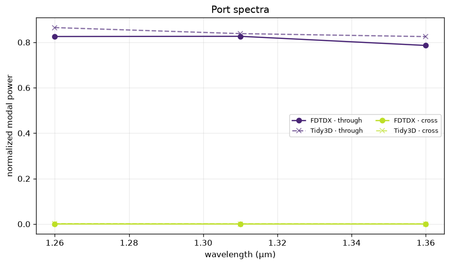
| wavelength_um | through | cross | monitored_total | relative_port_std | |
|---|---|---|---|---|---|
| 0 | 1.26 | 0.825490 | 0.000147 | 0.825637 | 0.999644 |
| 1 | 1.31 | 0.826373 | 0.000015 | 0.826387 | 0.999965 |
| 2 | 1.36 | 0.786148 | 0.000003 | 0.786151 | 0.999992 |
Reproduce and refine#
The notebook output above is retained from a real local execution. For a scientific
result, rerun after reducing spec.dl_um, increasing the time ceiling, and checking
port placement. The benchmark command below applies the catalog’s frozen-reference
tolerances and records the result in progress.json.
print("uv run fdtdx-bench run --case device_waveguide_crossing")
uv run fdtdx-bench run --case device_waveguide_crossing