Grids and boundaries#
The grid decides what geometry the solver can resolve; boundaries decide what physical world surrounds the finite array. They should be designed together.
Grid choices#
UniformGridOne spacing in all directions. It gives predictable numerical dispersion and remains useful for convergence studies and compact scenes.
RectilinearGridExplicit edge arrays on each axis. It concentrates cells near devices while allowing a coarser exterior. The update uses local metric factors, so sources, curl terms, and integrated detector quantities must all use the same cell measures.
QuasiUniformGridA convenience for gently varying resolution while limiting abrupt cell-size changes.
Resolve the smallest wavelength and the smallest geometry that matters. A 100 nm gap can control a coupling coefficient even when the wavelength is 1.55 µm.
Extruded 2-D domains#
If every material, source profile, and requested observable is translationally invariant along a periodic axis, represent that axis with one cell instead of advancing several identical planes. This is an exact reduction of the invariant Maxwell subspace; keep the same in-plane spacing and, when comparing against an existing discretization, choose courant_factor so the timestep is unchanged. A mode plane then has two one-cell dimensions (its normal and the invariant axis), so set fixed_propagation_axis on ModePlaneSource and ModeOverlapDetector. FDTDX solves the port mode on a non-degenerate virtual extrusion spanning the same physical thickness, collapses it back to one cell, and normalizes power on the actual detector plane.
Do not use this reduction for finite-height slabs, out-of-plane radiation, asymmetric claddings, oblique Bloch phase, or any source/material variation along the collapsed axis.
Automatic grid policy for devices#
The real-device runners choose a baseline pitch from two constraints:
where \(f_\min\) is the smallest gap, tooth, taper tip, or layer that materially affects the observable. In the current ladder, \(N_\lambda\) is approximately 15–20 in silicon and \(N_f\) is normally at least 4. Long adiabatic devices may use a coarser propagation-axis step while preserving transverse gap and layer resolution.
auto_interface_aligned_grid(shape, target_spacing, interfaces=...) partitions
each axis so every declared planar material transition is an exact grid face
while no cell exceeds the requested pitch. It also refuses a requested grid
above an explicit voxel budget. auto_pml_layers(physical_thickness, spacing)
converts a physical absorber thickness to per-axis layer counts, so refining a
mesh does not accidentally shrink the PML in micrometers.
This is a starting policy, not a convergence certificate. A production result should still be repeated at a finer grid. The important usability rule is that mesh choice is made from physical scales before looking at parity error; a benchmark should not acquire an arbitrary private mesh solely to chase its reference curve.
Touching polygons are boolean-unioned before rasterization. Otherwise two mathematically connected pieces can snap to different cells and leave a one-cell seam—a large perturbation in a 150–200 nm coupler gap or a narrow grating tooth.
Boundary families#
Boundary |
Physical model |
Typical use |
|---|---|---|
PML |
lossy coordinate stretch that absorbs outgoing waves |
open radiation and waveguide ports |
Periodic |
opposite faces repeat with zero phase shift |
unit cells and effectively 2D reductions |
Bloch |
opposite faces differ by a prescribed phase |
oblique periodic excitation and band structure |
PEC |
tangential electric field vanishes |
ideal electric conductor or symmetry plane |
PMC |
tangential magnetic field vanishes |
magnetic symmetry plane |
BoundaryConfig and boundary_objects_from_config build consistent face objects and their placement constraints.
PML practice#
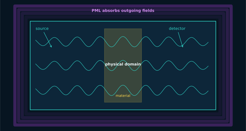
Leave separation between the source/device and PML; near fields are not plane outgoing waves.
Increase thickness before assuming a material or source is unstable.
Continue every guided structure through the outer PML boundary; terminating a high-index guide just before or inside the absorber creates a reflector.
Validate decay by monitoring residual field energy after the source turns off.
Automatic runtime cutoff#
Broadband device runs have a conservative maximum time window and a shared relative-energy exit test. The source first turns off; the solver then tracks residual field energy and stops only after it remains below the declared fraction of peak energy for the required hold interval. This gives long-lived multimode and resonant tails time to decay without forcing every ordinary waveguide run to consume the full window.
The maximum step count, actual step count, and final energy ratio are recorded in progress.json. Resonance extraction is different: the nanobeam case deliberately retains its ringdown because that decay rate is the measured quantity.
Symmetry#
Mirror symmetry reduces memory and compute only if geometry, material tensors, sources, and the requested mode have compatible parity. The fork supports field unfolding so reduced simulations can be interpreted on the full domain. Always compare a small symmetric scene with and without reduction before applying it to an optimizer.